• IP addresses are NOT logged in this forum so there's no point asking. Please note that this forum is full of homophobes, racists, lunatics, schizophrenics & absolute nut jobs with a smattering of geniuses, Chinese chauvinists, Moderate Muslims and last but not least a couple of "know-it-alls" constantly sprouting their dubious wisdom. If you believe that content generated by unsavory characters might cause you offense PLEASE LEAVE NOW! Sammyboy Admin and Staff are not responsible for your hurt feelings should you choose to read any of the content here.

    The OTHER forum is HERE so please stop asking.

ABNN Intel is fucked Technology Still @ Serangoon Tekka Era 10nm! AMD ROCKS @Computex2019

motormafia

Alfrescian
Loyal


https://www.pcworld.com/article/3397787/amd-ryzen-9-cpu-radeon-rx-5000-series-graphics-cards.html


News
AMD flexes 7nm muscle with a 12-core Ryzen 9 CPU and Radeon RX 5000 graphics cards
AMD challenges Intel and Nvidia with more efficient CPUs and GPUs, including our first look at the "Navi" brand and some great next-gen Ryzen parts.


By Gordon Mah Ung

Executive Editor, PCWorld | May 26, 2019 08:31 PM PT


su-on-7-nm-real-100797551-large.jpg
Mark Hachman / IDG


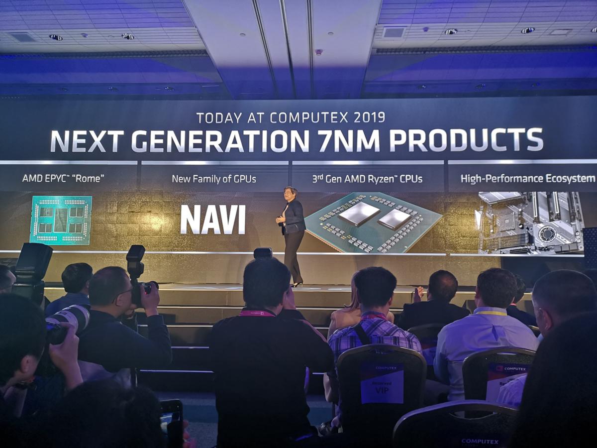
The coremageddon has begun: AMD Monday dropped its long-awaited 12-core Ryzen 9 3900X at Computex on Monday, saying that it will outpace Intel’s 12-core CPUs for almost a third to half the price—and that’s just an inkling of AMD’s 7nm onslaught against Intel and Nvidia.
"To be a technology leader, you have to make big bets," said Lisa Su, AMD's chief executive, speaking at her first Computex keynote. AMD's biggest bet was in developing its chips for 7nm, and those bets are beginning to pay off.
During the kick-off keynote for Computex, AMD CEO Lisa Su unveiled:


[ Further reading: Best graphics cards for PC gaming ]
  • “RDNA,” AMD’s new graphics architecture brand for its next-gen "Navi" core, which will be called the Radeon RX 5700 graphics card and go head-to-head with Nvidia’s GeForce RTX 2070.
  • An 8-core, 16-thread Ryzen 7 3700X with stupidly good power efficiency of 65 watts.
  • An 8-core, 16-thread Ryzen 3800X that all but erases any gaming deficits the CPUs have had versus the Intel competition.
  • The world’s first PCIe 4.0-ready PC parts
  • A dual-processor “Rome” Epyc server running laps on a dual-processor Intel Xeon Platinum 8280 server.
The most anticipated news, though, was AMD's Ryzen 9 3900X CPU. Su said the 12-core Ryzen 9 will have a boost clock of 4.6GHz with a base clock of 3.8GHz. The Ryzen 9 3900X will also pack in 70MB of cache and cost just $499.
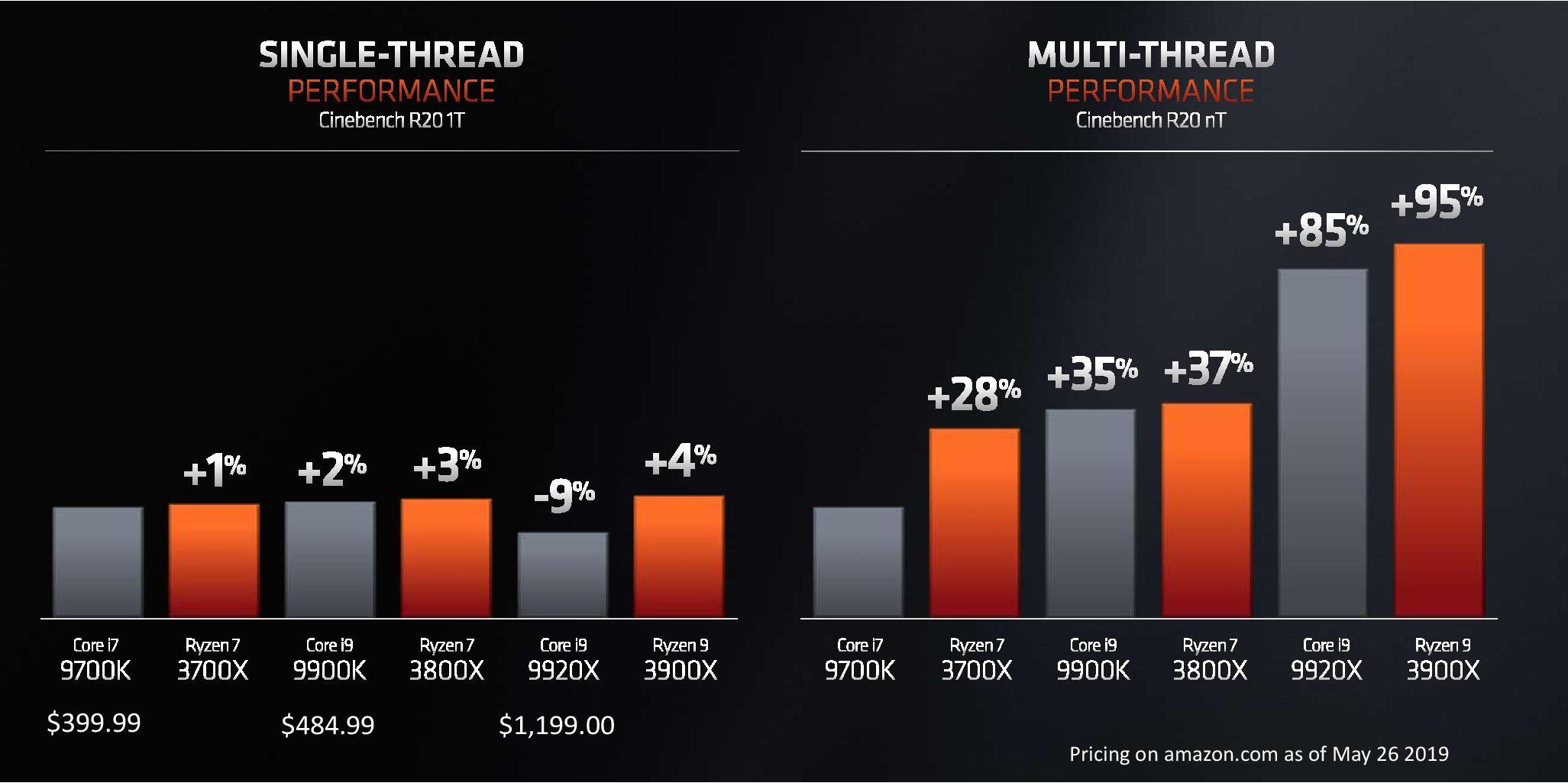
That's incredibly aggressive, especially when you consider that rival Intel wants $1,199 for its 12-core Core i9-9920X. Intel's core-count per dollar value looks even worse when you consider that AMD claims the Ryzen 9 3900X will outperform it by 14 percent in single-threaded tasks in Maxon’s new Cinebench R20 and 6 percent in multi-threaded tasks. It’s not just Cinebench R20 either. During the keynote, Su showed the Ryzen 9 3900X throwing down with $1,199 Core i9-9920X in a Blender demonstration too.
Even more impressively, the Ryzen 9 3900X will do it with a TDP rating of 105 watts, while the 14nm-based Core i9-9920X has a TDP of 165 watts. That’s not even mentioning that AMD typically measures its maximum thermal dissipation on a worst-case scenario while Intel’s TDP ratings shy toward what it calls normal use. Intel CPUs often exceed their formal TDP.
"We were not satisfied," Su said of the second-generation Ryzen. "Our engineering teams wanted to do more."
ryzen_3000_1-100797540-large.jpg
Gordon Mah Ung
The new Ryzen 3000 chips will features PCIe 4.0 support. When combined with a PCIe 4.0 GPU and X570 motherboard, you can build an all PCIe 4.0 system.
The Ryzen 7 3700X’s TDP is just as stunning though. With 8-cores and 16-threads, it’ll produce just 65W of heat and hit a boost clock of 4.4GHz with a base clock of 3.6GHz. A comparable 8-core, 8-thread Core i7-9700K will put out 95 watts (and often exceed that).

While Su didn’t detail where all of the added performance comes from, a lot probably comes from the increased efficiency of the CPU. It had been rumored that the new Zen 2 cores would offer a very impressive 15 percent increase in Instructions Per Clock (or IPC). That rumor turned to be correct, as Su confirmed that the Zen 2 cores are 15 percent more efficiency the previous Zen cores.
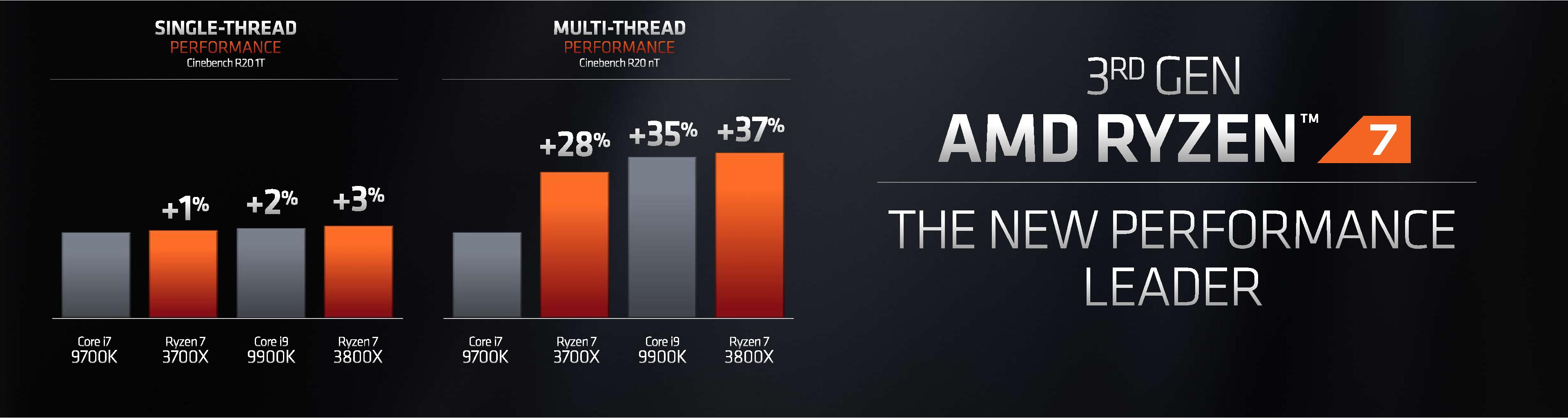
Compared to the 95W Core i7-9700K, Su said the 65 watt Ryzen 7 3700X will outperform it by about 1 percent in single-threaded tasks (again using Cinebench R20 as the yardstick) and a smoking 28 percent in multi-threaded tasks. If you’re not impressed by a 1 percent performance difference, remember the Ryzen 7 3700X has a maximum boost clock speed of 4.4GHz while the Core i7-9700K’s Turbo Boost speed is 4.9GHz. And yes, the Ryzen 7 3700X is lower in cost too, with a list price of $329 compared to the $385 for the Core i7-9700K.
If you want to burn a little more power and create a little more heat, Su also teased a second Ryzen 7 3800X that pushes the TDP up to 105 watts. That takes the boost clock to 4.5GHz and the base clock to 3.9GHz.
Although AMD's Su didn't mention them in her keynote, AMD also announced several new Ryzen chips: the 8-core, 16-thread Ryzen 7 3800X (3.9GHz base/4.5GHz boost, 105W, $399); the 6-core, 12-thread Ryzen 5 3600X (3.8GHz base/4.4GHz boost, 95W, $249); and the 6-core, 12-thread Ryzen 5 3600 (3.6GHz base/4.2GHz boost, 65W, $199).
Ryzen’s gaming deficit looks to be erased
Compared to the fantastic Ryzen 7 2700X, the Ryzen 7 3800X has a 34 percent higher frame rate in League of Legends and Counter Strike: Global Offensive, AMD said. In PlayerUnknown’s Battlegrounds, it’s about 22 percent faster, with Overwatch coughing up 21 percent higher frame rates. AMD also said Dota 2 is 15 percent faster and Grand Theft Auto V is about 14 percent faster on the Ryzen 7 3800X.
AMD didn’t share comparisons against an Intel CPU, but with that sort of frame rate increase, it looks like one of the penalties AMD’s Ryzen chips have long held against Intel CPUs at lower resolutions might be nearly non-existent now (assuming AMD’s numbers come courtesy of a system with a fast GPU like the GeForce RTX 2080 and a common 1080p resolution).
The Ryzen 7 3800X offers about three percent more performance in single-threaded tasks than a Core i7-9700K and about 37 percent increased performance in multi-threaded tasks, AMD said.
But that’s not the CPU that AMD probably wants you compare the Ryzen 7 3800X against. That’s because Su also showed off the Ryzen 7 3800X outperforming Intel’s vaunted 8-core, 16-thread Core i9-9900K by about 1 percent in single-threaded tasks and about two percent in multi-threaded tasks. The Ryzen 7 3800X costs $399 though, while Intel’s Core i9-9900K tilts it at $484 or more on the street.
Why not show the $499 Ryzen 9 3900X against the $484 Core i9-9900K? We’d guess there’s a bit of gamesmanship there. While the 12-core Ryzen 9 3900X should easily clean Intel’s clock on multi-threaded tasks, it would also probably lose ground in single-threaded tasks. Of course, they’re both about the same price so it’s probably a wash. (AMD likely gives you a cooler too.)
Winning the race to PCI Express 4
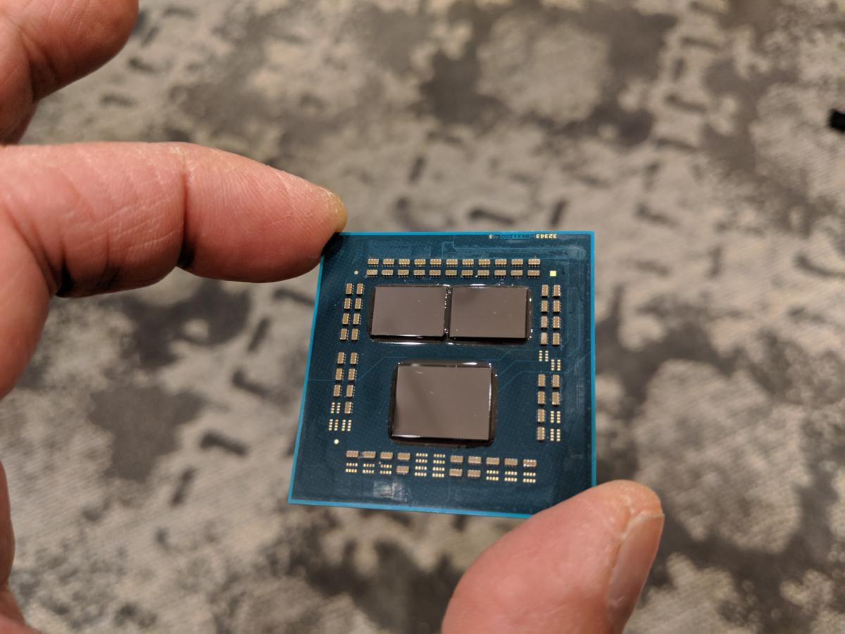
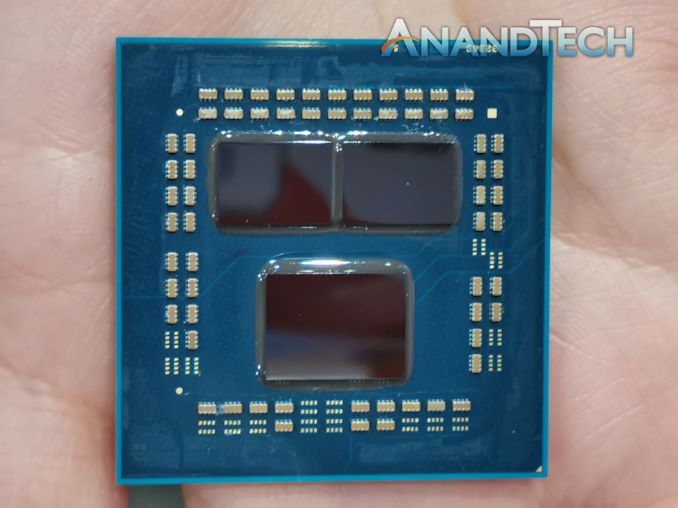
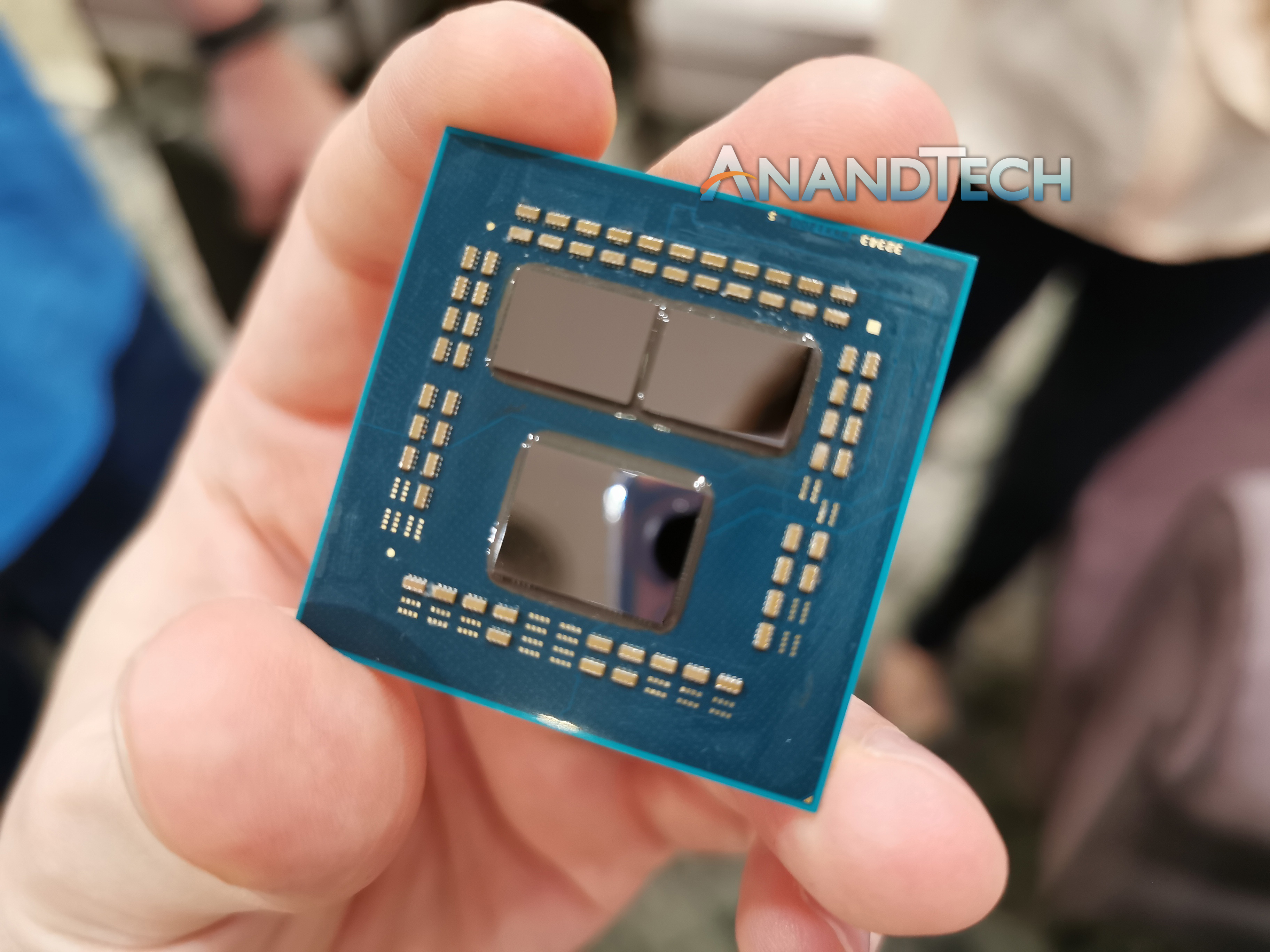
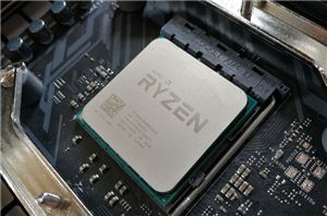
Under the heat spreader, AMD officials told us the 12-core Ryzen 9 will be built using two Client Computing Devices (or CCDs) while the two 8-core Ryzen 7 chips will be built using single CCDs. The CPU is said to have 40 PCIe lanes. How that’s counted up isn’t clear, but it may also count up PCIe lanes in the new X570 chipset too. For its part, Asus appeared on stage to announce that it will have over 30 X570 boards.
We’re still looking for clarity but we’d guess that AMD is counting lanes located in the chipset controller, which typically aren’t as “good” as PCIe lanes in the CPU. We’ll update our story once we have more details.
Still, even if they’re in the chipset, they’re still PCIe 4.0 lanes though, right? To that point, AMD said with the PCIe 4.0 support in the new Ryzen chips, combined with the PCIe 4.0 in X570 motherboards, plus the PCIe 4.0 in its new Radeon RX 5700, you basically have all the makings of the “world’s first PCIe 4.0-ready gaming PC.”
Company officials are quite proud of that fact because it basically means that AMD already crossed the PCIe 4.0 finish line before Intel and Nvidia appear to even care to enter the race.
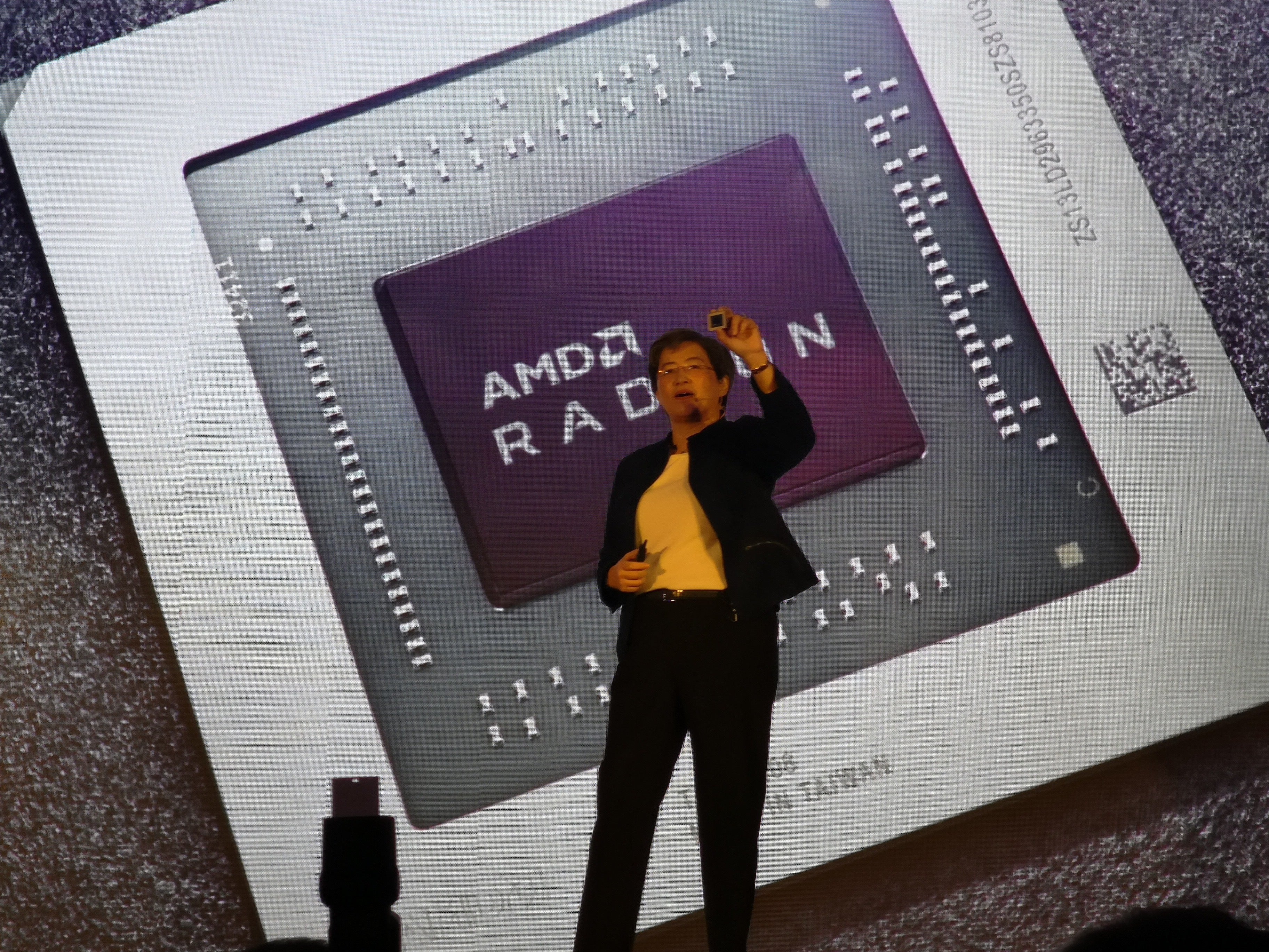
A 7nm Radeon RX 5700 too?


Gordon Mah Ung
AMD’s new Radeon RX 5000-series of GPUs will offer 25 percent better performance per clock and 50 percent better performance per watt, the company said.
With Ryzen out of the way, AMD also teased its long-awaited “Navi” graphics architecture. According to Su, over 400 million gamers use the Radeon brand, from consoles to PCs to the data center.
RDNA, though, was created with the same thinking that powered the Zen brand: a ground-up rebranding for an entirely new architecture, Su said.
Su said its first 7nm Navi implementation will be part of the first Navi card: the Radeon RX 5000 family (with the 50-00 name deriving from the company’s milestone anniversary this year). The first GPU to hit the road will be the Radeon RX 5700, which will go toe-to-toe with Nvidia’s GeForce RTX 2070. As AMD’s first 7nm GPU, Su said the card will hit higher clock speeds and use less power than the current Radeon generation.


Mark Hachman/IDG
With a multi-level cache hierarchy, the Radeon RX 5700 offers greater bandwidth too. Su said the new Radeon RX 5000-series cards and their RDNA GPU architecture will offer 25 percent greater performance per clock and 50 percent greater performance per watt than its previous Vega-based cores. AMD also showed off a "preview" of Navi outperforming an RTX 2070 on Strange Brigade.
If you’re thirsty for more details on the Radeon RX 5700, you probably won’t have to wait much longer. Su said the Radeon RX 5700 cards should be available by July, and the company is holding an event at the annual E3 gaming show on June 10, where we’d expect to hear more details, including pricing, about Navi’s consumer form.
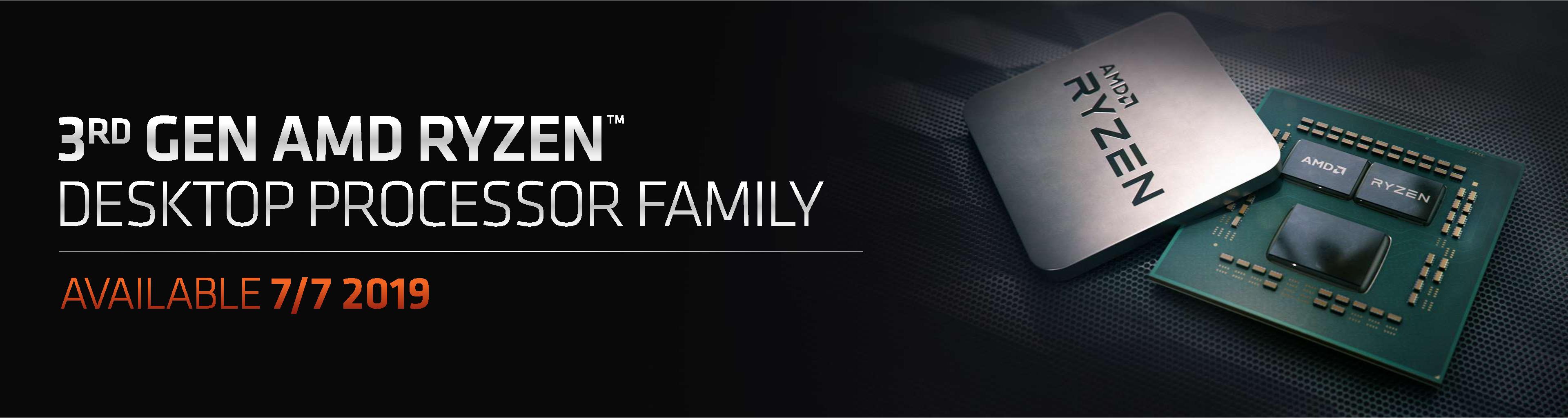
And yup, that July launch is on purpose. AMD said the new Ryzen processors are expected to be available on July 7 (psst, July is the 7th month) because, well, 7nm. As the first major chipmaker shipping 7nm chips to the public, AMD might as well rub it in.


To comment on this article and other PCWorld content, visit our Facebook page or our Twitter feed.


Related:


https://www.anandtech.com/show/1440...-cores-for-499-up-to-46-ghz-pcie-40-coming-77


AMD Ryzen 3000 Announced: Five CPUs, 12 Cores for $499, Up to 4.6 GHz, PCIe 4.0, Coming 7/7
by Ian Cutress on May 26, 2019 11:30 PM EST

171 Comments + Add A
Comment


Ryzen9_3800X_Car_678x452.jpg


Today at Computex, AMD CEO Dr. Lisa Su is announcing the raft of processors it will be launching on its new Zen 2 chiplet-based microarchitecture. Among other things, AMD is unveiling its new Ryzen 9 product tier, which it is using for its 12-core Ryzen 9 3900X processor, and which runs at 4.6 GHz boost. All of the five processors will be PCIe 4.0 enabled, and while they are being accompanied by the new X570 chipset launch, they still use the same AM4 socket, meaning some AMD 300 and 400-series motherboards can still be used. We have all the details inside.
A lot of people have been after details about AMD’s next generation Ryzen platform for several months, ever since AMD teased the Matisse Ryzen 3000 design at CES back in January. Most of that information is coming out today, with Ryzen 9, Ryzen 7, and Ryzen 5 processors in the mix. All of these processors will be officially launched on July 7th (which is 7/7), correlating with the fact that the core chiplets of these products are built on TSMC’s 7nm process. This is technically a Sunday, but AMD doesn’t mind too much. In reality, it means users might even get them in the mail on the following Monday.
Before talking about features, let’s go straight into the CPU list, as that’s what most of you are here for.
AMD 'Matisse' Ryzen 3000 Series CPUsAnandTechCores
ThreadsBase
FreqBoost
FreqL2
CacheL3
CachePCIe
4.0DDR4TDPPrice
(SEP)Ryzen 93900X12C24T3.84.66 MB64 MB16+4+4?105W$499Ryzen 73800X8C16T3.94.54 MB32 MB16+4+4?105W$399Ryzen 73700X8C16T3.64.44 MB32 MB16+4+4?65W$329Ryzen 53600X6C12T3.84.43 MB32 MB16+4+4?95W$249Ryzen 536006C12T3.64.23 MB32 MB16+4+4?65W$199
The New Flagship: Ryzen 9 3900X
The Ryzen 3000 series will debut a new product tier for AMD: Ryzen 9. In this case, the Ryzen 9 3900X will be AMD’s first mainstream desktop 12-core processor. The processor is the only one of the group that uses two chiplets, in a 6+6 configuration. The 3900X will have a base frequency of 3.8 GHz, a turbo frequency of 4.6 GHz, and line up with 6 MB of L2 cache and 64 MB of L3 cache. This confirms that each chiplet has 32 MB of L3 cache, doubling what we saw on the first generation of the Zen microarchitecture. This CPU has a TDP of 105W, which for AMD processors is usually a good measure of all-core power consumption, and will be enabled with 24 PCIe 4.0 lanes (16 for GPU, 4 for storage, 4 for the chipset).
AMD 'Matisse' Ryzen 3000 Series CPUs
Ryzen 9AnandTechCores
ThreadsBase
FreqBoost
FreqL2
CacheL3
CachePCIe
4.0DDR4TDPPrice
(SEP)Ryzen 93900X12C24T3.84.66 MB64 MB16+4+4?105W$499
The Ryzen 9 3900X will have a suggested e-tail price of $499, and it will come with a cooler (more details in the coming weeks). AMD compared this processor in its presentations to Intel’s 12-core HEDT processor, the Core i9-9920X, which has an MSRP of $1199 and doesn’t come with a cooler.
In this comparison, AMD provided Cinebench R20 performance data comparing the two processors (it should be noted that we can’t confirm these results at this time). AMD states that in single thread performance, the 3900X beats the 9920X by +14%, and also wins in multi-threaded performance by 6%, all while having a lower TDP (165W vs 105W).

The Ryzen 9 3900X is the new mainstream desktop flagship, although AMD clearly has enough headroom on this design to enable a full 16 cores. Most users will expect this to come in the future, so it will be interesting to see if AMD will strategically play this card.
Mainstream Madness: Ryzen 7 at 65W
For the Ryzen 7 lineup, AMD is keeping this for the 8-core versions. These CPUs only have a single chiplet inside, and no dummy chiplet. Of the two CPUs in this segment, the one that gets a big shock from us is actually the cheaper model.
AMD 'Matisse' Ryzen 3000 Series CPUs
Ryzen 7AnandTechCores
ThreadsBase
FreqBoost
FreqL2
CacheL3
CachePCIe
4.0DDR4TDPPrice
(SEP)Ryzen 73800X8C16T3.94.54 MB32 MB16+4+4?105W$399Ryzen 73700X8C16T3.64.44 MB32 MB16+4+4?65W$329
The Ryzen 7 3700X is an eight core, sixteen thread CPU with a 3.6 GHz base frequency and a 4.4 GHz turbo frequency. It has 4 MB of L2 and 36 MB of L3 (half the L3 compared to Ryzen 9, because it only has one chiplet), but the amazing thing is that this chip has a TDP of just 65W. Just on paper, it looks like this processor is one of the most efficient x86 performance desktop processors ever made. This is likely the CPU configuration that AMD used in its Cinebench R20 demo back at CES, where it showed R20 equivalent multithreaded performance for 40% less system power. And the price for all this performance? Only $329. If I put my reviewer hat on and look at these specifications at a high level, the Ryzen 7 3700X promises to be the mainstream chip of choice for a substantial number of high-performance PCs this year.
Like with the Ryzen 9 3900X, AMD also ran a Cinebench comparsion with the 8 core Ryzen 3700X versus Intel's mainstream Core i7-9700K. Here they scored 4806, verus 3726 for the 9700K in R20's multithreaded test.
The other CPU in this bracket is the Ryzen 7 3800X. This is going to be the direct upgrade from the current Ryzen 7 2700X, comes with eight cores and sixteen threads, with a base frequency of 3.9 GHz and a boost frequency of 4.5 GHz. It doesn’t seem overly impressive compared to the 3700X with its larger 105W TDP for only a few hundred MHz more on the base frequency, however as we’ve seen with the 2nd Gen Ryzen, that extra TDP headroom usually helps with technologies like XFR that manage the boost frequencies. AMD hasn’t said anything new about how XFR or Precision Boost works in the new generation yet, we have to wait until nearer launch for that information. However the extra frequency and extra TDP will cost an extra $70: the Ryzen 7 3800X will retail for $399.
Budget Builds: Ryzen 5 with Six Cores
Not mentioned during the keynote, but discussed in the press release, AMD also gave information about its new Ryzen 5 processors.
AMD 'Matisse' Ryzen 3000 Series CPUs
Ryzen 5AnandTechCores
ThreadsBase
FreqBoost
FreqL2
CacheL3
CachePCIe
4.0DDR4TDPPrice
(SEP)Ryzen 53600X6C12T3.84.43 MB32 MB16+4+4?95W$249Ryzen 536006C12T3.64.23 MB32 MB16+4+4?65W$199
These are still very competitive – users can now buy a six-core processor for under $200. The processor frequencies are consummate with the position in the stack, along with the pricing, and both CPUs will support all the same technologies (PCIe 4.0, etc) as the bigger chips. These chips still use a single chiplet, not a dual chiplet design.
Performance Numbers
AMD provided some performance numbers to compare AMD to Intel CPUs. All of these tests are using Cinebench R20, which should be noted is a floating point rendering test that AMD already does well on, but there aren’t any specific optimizations here for each CPU.

Direct chip to chip comparisons put AMD’s single thread performance against Intel at +1%. Though it should be noted here that something like the Ryzen 7 3800X, which boosts to 4.5 GHz, is being compared to an Intel CPU that boosts to 5.0 GHz. That would put IPC on this test firmly in the hands of AMD. Multi-threading results are a similar scenario, although the margin of difference tends to drop the more cores that AMD has access to, perhaps because more cores are fighting to get to the memory with a slightly extended memory latency compared from Intel.
Comparing Zen 1 to Zen 2, AMD is promoting that the Ryzen 9 3900X offers +32% better single threaded performance over the Ryzen 7 1800X. Given that we saw a 40-52% IPC increase from pre-Zen to Zen 1, another +32% on single threaded performance is a good amount to have, although that 32% does include frequency uplift. When we get the chips in, we’ll do an obvious comparison test to find the IPC difference. In multi-threaded results, AMD is promoting +100% multithreaded performance, which is helped by +50% more cores, 2x better FP throughput per core, and higher frequencies.
Other Features and X570 Motherboards
Aside from the 7nm chiplets, and the monumental price comparison to Intel, there are some other features to mention. AMD is promoting a +15% direct IPC increase from Zen 1 to Zen 2, due to microarchitecture improvements and cache size doubling on the L3. The CPU has 24 PCIe 4.0 lanes: sixteen for the GPU (or other PCIe cards), four for storage, and four for the chipset. The four for storage will likely be linked to the top M.2 slot. Given that some companies are advertising PCIe 4.0 SSDs here at Computex, we expect more to follow in due course.
The new X570 chipset has 16 lanes, four for the upstream connection to the CPU, and twelve downstream for other devices. There is some discontinuity here – we heard from partners that AMD actually removed four PCIe lanes from the chipset design in order to bring the TDP of the chipset down from 15W to 11W; but the full-fat 15W version will be on the next editions of the high-end desktop (which would suggest that Threadripper isn’t dead, contrary to a lot of reporting – this is a question we will be asking Lisa Su later today). We have already seen a number of X570 motherboards ready to enter the market, and we expect around 25 new X570 models in total. It is clear that motherboard manufacturers are now getting serious on AM4 – some of these boards are likely to retail up to $600. These manufacturers are clearly expecting AMD to hit Intel hard, and have designed the motherboards to match the best that they make for Intel's CPUs.
One bit of information not disclosed is memory support, however given our discussions with AMD’s partners, this is likely to be DDR4-3200 in one module per channel mode. This is a small bump over 2nd Gen Ryzen, but still a welcome one. It will be interesting to see how the memory controller works on this design for pushing that frequency. The memory frequency and Infinity Fabric frequency are still linked as before, so bumping up the memory frequency has additional benefits.
Finally, the release date for all these CPUs is going to be July 7th. We’re waiting on AMD to disclose the sampling time frame, but our aim is to get our review up on day one. Suggestions for the review are most welcome.
We also have access to Dr. Lisa Su directly after the keynote today, and will write up our Q&A in due course. Stay tuned for that.
Want to keep up to date with all of our Computex 2019 Coverage?
Laptops
Hardware


https://sea.ign.com/pc/149612/news/amd-announces-next-gen-gpus-and-cpus-at-computex


PC / May 28, 2019
AMD Announces Next-Gen GPUs and CPUs at Computex


Navi and 3rd Gen Ryzen coming soon.
By Josh Norem
At Computex AMD has pulled the wraps off its next-gen GPU and CPU architectures, revealing its Navi GPU and third generation Ryzen CPUs as well. AMD CEO LIsa Su delivered a keynote address to kick off the hardware-focused trade show in Taipei, and showed off some of its upcoming hardware, with the promise of going more in-depth at E3 in two weeks time.
AMD Introduces Navi
The existence of AMD's Navi GPUs has never been a secret, but up until now all we knew about them was that they were going to be built on a 7nm node. It's such a non-secret that Sony has already stated it will be using Navi in the next-gen Playstation. At Computex, Su revealed the GPUs in the Navi lineup will be called the Radeon 5000 series; a nod to the company's 50th anniversary. They will also be the first GPUs built on a new RDNA microarchitecture (short for Radeon DNA), which is a departure from the previous GCN architecture that has powered everything from Hawaii up to Vega and the current Polaris cards. AMD announced it as the RX 5700 series, but pricing, clock speeds, and pricing were all TBD. However, they did say the GPUs will be available in July.
Screen-Shot-2019-05-27-at-9.37.14-AM.png

Dr. Su held up a Navi chip and pointed out that it was indeed a small chip, but said small is good and pointed to the fact that AMD is focusing on reduced power consumption; a pain point of previous AMD GPUs compared to Nvidia chips. As far as performance goes the company showed a demo of Strange Brigade running alongside an Nvidia RTX 2070, and noted the Navi chip was running ten percent faster. The RX 2070 is a $500 GPU, so if Navi comes out for $300 or so, that will indeed be quite an achievement. In a roundtable after the keynote AMD said it's not ruling out support for ray tracing, and that more info will be coming in June.
Screen-Shot-2019-05-27-at-9.43.13-AM.png

Dr. Su also pointed out that Navi GPUs are the first GPUs to use a PCI Express 4.0 interface, which double the amount of bandwidth compared to PCIe 3.0 GPUs we are all using now. Of course, to get access to that bandwidth you also need a motherboard and CPU that supports PCIe 4.0, which AMD announced as well.
3rd Gen Ryzen CPUs
The existence of 3rd gen Ryzen chips was also not a secret, but like the GPUs, we didn't know much about them other than their name. Dr. Su revealed these chips will use a new second-generation design that will offer a 15 percent instruction per clock (IPC) uplift compared to previous Ryzen chips. The first chip announced is the Ryzen 7 3700X, which is a 7nm CPU with 8-cores and 16-threads, running at 3.6GHz base clock with a 4.4GHz boost clock and surprisingly low 65w TDP. The company showed a demo of it running Cinebench R20 faster than the Intel Core i7 9700K, which is an eight-core/eight-thread CPU with a 95w TDP. The company spokesman said it was running "1/3 faster" than the Intel chip. Su said compared to the Intel chip, 3rd gen Ryzen would be "similar" in single-threaded performance, but approximately 28 percent faster in multi-threaded workloads. AMD announced the price of the 3700X at $329.
Screen-Shot-2019-05-27-at-10.04.10-AM.png

Lisa Su also announced the Ryzen 3800X, which is a 105w TDP GPU like the Intel 9700K. The company compared it to the i7 9900K in PUBG, and said it basically performs exactly the same. Previous AMD GPUs were mostly considered slightly inferior to Intel's chips when it comes to gaming, so AMD is looking to change that with its new CPUs. The 3800X will sell for $399.
Lisa Su also had a "one more thing" moment, and saved the best for last by announcing the Ryzen 9 series chips. This will be the first "mainstream" CPU with 12 cores and 24 threads running at 4.6GHz boost, all at 105w TDP. Dubbed the 3900X, AMD showed it running Blender much faster than the Intel Core i9 9920X HEDT chip, which is a 165w chip that sells for over $1,000. The AMD CPU ran the Blender demo 18 percent faster than Intel's chip, and will be priced at $499, severely undercutting Intel's pricing model in this segment. All of the new Ryzen processors will go on sale July 7th.
Screen-Shot-2019-05-27-at-10.23.32-AM.png

Stay tuned for more details on all the new AMD hardware, as much more should be revealed at E3 in a few weeks.
Josh Norem is IGN's Executive Editor for Tech. When he's not upgrading his PC he's trying to get his foster kittens adopted.


Share Tweet Submit
 

motormafia

Alfrescian
Loyal
This is ABNN Intel for you, fuck away your security YET AGAIN! & if you try to fix it, it further set you back at 40% speed performance lost PERMANENTLY!
INTEL = Serangoon Tech!


https://venturebeat.com/2019/05/14/...es-os-patches-with-up-to-40-performance-hits/


Intel ZombieLoad flaw forces OS patches with up to 40% performance hits

Jeremy Horwitz@horwitz May 14, 2019 11:58 AM

intel-i91-e1557860193459.jpg

Above: Intel's latest chips.
Image Credit: Intel


When security researchers disclosed a series of major vulnerabilities impacting Intel processors back in January 2018, it was clear that “Meltdown” and “Spectre” were indeed serious — and wouldn’t be the only exploits of multi-threading chips. Now a new Intel chip vulnerability nicknamed “ZombieLoad” has been revealed to the public, and though it’s already being patched by three major operating system makers, there’s some bad news: full protection could reduce your CPU’s performance by up to 40%.
Referred to by the more technical name “Microarchitectural Data Sampling,” the ZombieLoad exploit enables an attacker to access privileged data across trust boundaries. In a cloud hosting environment, it could enable one virtual machine to improperly access information from another; researchers also showed that it could be used for app surveillance and password acquisition. The vulnerability broadly impacts operating systems that run on Intel chips, including Android, Chrome, Linux, macOS, and Windows.
Recommended videos
Powered by AnyClip


In a just-published support document, Apple suggests that full ZombieLoad mitigation will require Intel chip users to disable Intel’s hyper-threading processing feature — a major selling point of the chipmaker’s CPUs. During testing this month, Apple says that it found “as much as a 40 percent reduction in performance with tests that include multithreaded workloads and public benchmarks,” though actual performance impacts will vary between machines.

Because of that steep performance drop, Apple has implemented a partial mitigation in macOS Mojave 10.14.5, leaving users to decide whether they want to disable hyper-threading for full protection. If so, the support document provides Terminal commands to turn the feature off and on, notably including a requirement that the machine boot in recovery mode to disable the chip feature.

Google and Microsoft (via TechCrunch) have also started the process of patching their Intel-based operating systems. In Google’s case, Chrome OS devices have already received some protections and will receive more in the next OS release; Intel-only Android devices are rare, but will receive OS patches once device makers deploy them. Microsoft is releasing patches for Windows today, and has already protected Azure users. Some microcode processor updates will come from Microsoft directly, and others from device makers.

The ZombieLoad issue was apparently disclosed to Intel one month ago, and impacts all Intel processors produced since 2011. Chips from AMD and ARM are not believed to be susceptible to this flaw. According to vendors, there are no known real-world exploits of the vulnerability at this point, though the researchers simply say that they don’t know if it’s been abused in the wild.

Update at 12:45 p.m. Pacific: An Intel page discussing the vulnerabilities downplays the performance impacts, suggesting that the performance impact is small: up to 3% without disabling hyper-threading, and up to 8-9% with hyper-threading disabled, though included charts show tinier changes using the latest, high-end Intel Core i9-9900K processors.

Intel underscores that disabling hyper-threading isn’t really necessary for some users: consequently, unless it’s necessary for a given customer’s workloads and security environment, it says that it’s “not recommending that Intel HT be disabled, and it’s important to understand that doing so does not alone provide protection against MDS.”
 

syed putra

Alfrescian
Loyal
CEO of amd is lisa su from tsiwan. Cannot match intel's indian chief engineeting officer dr Venkata Murthy Renduchintala. Once companies got blacks, it won't look at your backs.
 

Tony Tan

Alfrescian
Loyal
5nm chip is coming to an iPhone near you, thanks to TSMC.

https://www.tomshardware.com/news/tsmc-5nm-euv-process-node,38995.html

Taiwanese TSMC only depending on Chow Ang Moh semicon lithographic machines like ASML. Taiwanese cannot make their own machine, this type of position is 做牛做马做奴才(奴隶) it is alike the 郭台铭‘s factories of Foxcon building gay phones for Ang Moh. Essentially just providing labor cheaply, operating Chow Ang Moh's Machines, while Chow Ang Mohs relax drink beer and enjoy cheap products.

Chinese now are cannibalizing Chow Ang Moh. Chinese designed own CPUS & CHIPS and own Lithographic Machines. Defined own new standard put Chow Ang Moh very far lagging behind and cannot catch up. Ang Moh beggars can find no way to earn a single cent to pay debts. Print counterfeit dollars also won't work any more.


https://www.cnqiang.com/2019/04/49623.shtml


一不偷二不抢,我国半导体设计水平已达7nm,荷兰人:窃取技术

2019-04-14 10:36:31 | 来源: | 参与: 0 | 作者:本站原创


ASML光刻机
如果问这个世界上比印钞机更赚钱的机器是什么,那肯定是光刻机了。没有芯片就造不了手机,而光刻机是制造芯片的核心设备之一,也是我国受制于人的核心技术。都说顶级光刻机只有荷兰可以制造,前不久荷兰半导体设备制造商阿斯麦(ASML)出了件不大不小的事儿。
如果把这事和最近我国工信部发布的消息放一起看,就有些微妙了。前段时间深圳举行了2019年全国电子信息行业工作座谈会,工业和信息化部电子信息司集成电路处处长任爱光表示,我国的集成电路设计业产业规模在不断壮大,设计水平达到7纳米,不过还是以中低端产品为主,集成电路制造业,存储器工艺有所突破,14纳米逻辑工艺即将量产,虽然和国外还存在一定的差距,但在越变越好。
20190414103814625.png

图丨工信部电子信息司
荷兰公司出的事发生在这之后,据荷兰财经报纸《金融日报》称,ASML公司的中国员工窃取公司机密,导致公司损失数亿美元。ASML是全球最大半导体制造设备供应商,主要业务是生产光刻机,顶级光刻机几乎被ASML垄断。外交部例行记者会上,发言人陆慷表示,中国高度重视知识产权保护,中国的科技发展一不靠偷,二不靠抢,是中国人自己用智慧和汗水奋斗出来的。
对此有网友表示“如果光靠某个员工看一下光刻机就能窃取技术,那这光刻机技术也没什么技术含量,简直是国际笑话”。荷兰的光刻机,不是说靠荷兰一家就能搞定的,就拿光刻机中心的镜头举例,想要镜片材质做到均匀,需要几十年甚至上百年技术积淀。同样一个镜片,如果让不同的工人去磨,光洁度能相差十倍,德国抛光镜片工人往往是祖孙三代都在一家公司的同一个岗位。这真要窃取技术,岂不是欧洲国家都要去一遍?


ASML光刻机
十多年前,中国为了填补光刻机空白曾去德国进行考察,当时就有工程师说“给你们全套图纸,也做不出来”。图纸确实很重要,但光刻机这东西不比其他,细节上的要求特别多,一个小动作、一根光纤、一行软件编码,都会影响到整个系统,不是说随随便便就能把技术学去的。
中国科技发展迅猛,有跟跑的,有并跑的,还有领跑的,和顶级光刻机的差距主要是在时间上,几个月解决不了光刻机的问题,而发展光刻机需要培养人才,需要用五十年一百年的长远眼光去做这件事,去改变人。


https://www.chainnews.com/articles/838659360792.htm

国产光刻机的希望
半导体行业观察 · 2019年4月13日 00:00

收藏


来源:内容来自「国君电子王聪 / 张天闻」,谢谢。
编者按:
近日,关于 ASML 的一则流言的传出,又引起了国内对光刻机的关注。作为芯片产业的重要设备,光刻机的意义是不言而喻的。值着这个机会,我们在这里转载一份关于国产光刻机龙头——上海微电子的介绍,帮助大家对本土这个领域有更深的了解。
上海微电子是在国家科技部和上海市政府共同推动下,由国内多家企业集团和投资公司共同投资组建的高科技企业。
公司成立于 2002 年,主要从事半导体装备、泛半导体装备以及高端智能装备的设计制造销售,其中光刻设备是公司的主营业务。公司在光刻设备领域拥有全国最先进的技术。目前公司光刻机可以应用于集成电路产业链中晶圆制造、封装测试,以及平板显示、高亮度
LED 等领域。


1.2
公司在大陆市场份额高,业绩逐渐向好
公司是大陆光刻设备龙头企业。

目前公司所研发的高端前道光刻机实现 90nm 制程。在中端先进封装光刻机和 LED 光刻机领域,公司技术领先,在中国大陆市场份额已经超过 80%。其先进封装光刻机率先实现量产并远销海外市场,获得多项大奖和技术认证广受业内认可。根据芯思想数据,上海微电子 2018 年出货大概在 50-60 台之间。
根据中国半导体协会,公司在半导体设备商中排名第 5,是唯一上榜的专门研究销售光刻机的厂商。

7804678dbd8316432cc97b7f55c805c4.jpg

公司具有强大的研发团队,自主创新能力不断提升。
在国家的大力支持下,公司不断通过引进优秀的人才壮大核心团队以进一步提升公司的竞争力和产品研发效率。根据国投高新,上海微电子目前研发队伍不断壮大,其中包括拥有卓越才能的国家千人计划专家、上海市科技领军人才、上海市技术学科带头人等重量级专业人才。根据企查查数据,公司近年来专利发布数量呈增长态势,这也显示出上微自主创新能力不断提升。截至 2018 年 12 月,SMEE 直接持有各类专利及专利申请超过 2400 项,同时公司通过建设并参与产业知识产权联盟,进一步整合共享了大量联盟成员知识产权资源,涉及光刻设备、激光应用、检测类、特殊应用类等各大产品技术领域,全面覆盖产品的主要销售地域,使得公司竞争实力不断提升。公司是国家重点扶持企业。上海微电子在国家 02 专项的支持下积极布局光刻机制造。

上海微电子积极为 IPO 做准备。根据证监会公布的《上海微电子装备(集团)股份有限公司辅导备案基本情况表》,公司已经在 2017 年 12
月 27 日与中信建投证券股份有限公司签署辅导协议并进行辅导备案。
1.3
公司实控人是上海国资委
公司最大股东为上海电气,股本占比达到 32.09%。上海市国资委是公司的实际控制人,其通过电气集团、上海科投、泰力投资等股东合计持有公司
53.49% 的股权。公司拥有 4 家全资子公司以及一家参股子公司。

光刻机:高壁垒资本密集核心设备,市场广阔龙头集中
2.1
光刻技术是实现先进制程的关键设备
光刻机应用广泛,包括 IC 前道光刻机、用于封装的后道光刻机以及用于 LED 领域及面板领域的光刻机等等。

封装光刻机对于光刻的精度要求低于前道光刻要求,面板光刻机与 IC 前道光刻机工艺相比技术精度也更低,一般为微米级。IC 前道光刻机技术最为复杂,光刻工艺是 IC
制造的核心环节,利用光刻技术可以将掩模版上的芯片电路图转移到硅片上。光刻机是一种投影曝光系统,包括光源、光学镜片、对准系统等。在制造过程中,通过投射光束,穿过掩膜板和光学镜片照射涂敷在基底上的光敏性光刻胶,经过显影后可以将电路图最终转移到硅晶圆上。
0bb31d1c9ffc0b17d3a3423a6bddc074.jpg

光刻机分为无掩模光刻机和有掩模光刻机。
无掩模光刻机可分为电子束直写光刻机、离子束直写光刻机、激光直写光刻机。电子束直写光刻机可以用于高分辨率掩模版以及集成电路原型验证芯片等的制造,激光直写光刻机一般是用于小批量特定芯片的制造。有掩模光刻机分为接触 / 接近式光刻机和投影式光刻机。接触式光刻和接近式光刻机出现的时期较早,投影光刻机技术更加先进,图形比例不需要为 1:1,减低了掩膜板制作成本,目前在先进制程中广泛使用。随着曝光光源的改进,光刻机工艺技术节点不断缩小。
目前最先进的光刻机来自 ASML 的 EUV 光刻机,采用 13.5nm 光源,最小可以实现 7nm 的制程。
此设备的开发难度更高,使用条件更复杂目前只有 ASML 攻破此项技术。因为所有物质吸收 EUV 辐射,用于收集光(收集器),调节光束(照明器)和图案转移(投影光学器件)的光学器件必须使用高性能钼硅多层反射镜,并且必须容纳整个光学路径在近真空环境中,整个设备十分复杂。
3762fc1c3c19a8ac2e95825a5930f757.jpg

芯片尺寸的缩小以及性能的提升依赖于光刻技术的发展。
光刻设备光源波长的进一步缩小将推动先进制程的发展,进而降低芯片功耗以及缩小芯片的尺寸。根据 International Society for Optics
and Photonics 以及 VLSI Research 研究发现,高精度 EUV 光刻机的使用将使 die 和 wafer 的成本进一步减小,但是设备本身成本也会增长。
caaf1775d8e8fabca1e3e5d689652efd.jpg

563fc0ad11ae566bc73fe477b76119a4.jpg

目前光刻工艺是 IC 制造中最关键也是最复杂步骤,光刻机是目前成本最高的半导体设备,光刻工艺也是制造中占用时间比最大的步骤。
其约占晶圆生产线设备成本 30%,占芯片制造时间 40%-50%。以光刻机行业龙头 ASML 为例,其研发投入每年在 10 亿欧元左右,并且逐年增长。
高端 EUV 价格不断攀升。
根据芯思想,2018 年单台 EUV 平均售价 1.04 亿欧元,较 2017 年单台平均售价增长 4%。而在 2018 年一季度和第四季的售价更是高达 1.16 亿欧元。

ca38e498145b2644617873e35ce7b75f.jpg

2.2
光刻机市场空间广阔,高低端市场格局迥异
2.2.1. 光刻机市场龙头集中,中低端市场广阔竞争激烈
光刻机设备市场龙头集中,EUV 光刻机被 ASML 垄断。

全球光刻机出货量 99% 集中在 ASML,尼康和佳能。其中 ASML 份额最高,达到 67.3%,且垄断了高端 EUV 光刻机市场。ASML 技术先进离不开高投入,其研发费用率始终维持在 15%-20%,远高于 Nikon 和 Canon。


ASML 在高端 EUV、ArFi、ArF 机型市场占有率不断提升。
2017 年 ASML 上述三种机型出货量总计为 101 台,市场份额占比为 78.29%,到 2018 年 ASML 出货量增长到 120 台,市场份额约 90%
。2018 年 ASML 共出货 224 台光刻机,较 2017 年 198 年增加 26 台,增长 13.13%。Nikon2018 年度(非财年)光刻机共出货 106 台,半导体用光刻机出货 36 台,同比增长 33.33%,面板(FPD)用光刻机出货 70 台。2018 年 Canon 光刻机出货 183 台,同比增 1.6%。半导体用光刻机出货达 114 台,增长 62.85
%。但是主要是 i-line、KrF 两个低端机台出货,其面板(FPD)用光刻机出货 69 台。
IC 前道光刻机国产化严重不足。
目前国内光刻机处于技术领先的是上海微电子,其最先进的 ArF 光源光刻机节点为 90nm,中国企业技术整体较为落后,在先进制程方面与国外厂商仍有较大差距。

7e5f599f99efdea85ea8231389ebc816.jpg

Nikon 和 Canon 目前在高端市场技术与 ASML 相差甚远几乎完全退出市场,Canon 也退出了 ArF
光源光刻机研发与销售,将其业务重点集中于中低端光刻机市场,包括封装光刻机、LED 光刻机以及面板光刻机等,与复杂的 IC
前道制造相比,工艺要求和技术壁垒较低。
3fc102a8ec719a1bbeb2df99bc5e997b.jpg

封装光刻机技术不断发展,新技术不断涌现。
与前端区域相关。翘曲处理以及异质材料对光刻技术构成了巨大挑战。此外,一些 MEMS 制造设备需要精确的层层对准,步进和掩模对准器是目前大批量制造中使用的两种主要光刻技术。激光直接成像(LDI)和激光烧蚀等新的光刻技术也不断涌现。
中低端光刻机需求量不断增长,市场竞争加剧。
根据 Yole,2015-2020 年先进封装、MEMS 以及 LED 光刻机出货量将持续增长,预计到 2020 年总数将超过 250 台 / 年。中低端市场的不断增长主要受先进封装的推动,随着步进技术发展,2015 年到 2020 年先进封装光刻设备出货量年复合增长率达到 15%。MEMS 光刻市场主要受益于 IC 前道制造光刻机的重复使用与改装。中低端光刻机市场规模的不断扩大和相对于前道制造较低的技术壁垒,竞争者数目较多,目前尼康与佳能是中低端市场两大龙头。
a7aea9b5c1e9d3a5f43e18a6d6122ded.jpg

2.2.2. 半导体产线升级为光刻设备带来更大需求
晶圆尺寸变大和制程缩小将使产线所需的设备数量加大,性能要求变高。

12 寸晶圆产线中所需的光刻机数量相较于 8 寸晶圆产线将进一步上升,先进制程的发展将进一步提升对于光刻机性能的要求。
随着产业转移和建厂潮的推动和边际需求改善,光刻设备市场将不断增长。根据 Varianat Market
Research,到 2025 年全球光刻设备市场规模估计将达到 4.917 亿美元 ; 从 2017 年到 2025 年的复合年增长率将达到为 15.8%。

对接多元光刻机市场需求,积极开拓封装、LED 和平板显示光刻机业务
3.1
公司前道光刻机差距较大,后道封装光刻机优势明显
3.1.1. 公司前道光刻机与国际先进水平差距较大
公司 IC 前道光刻机技术与国际先进水平差距明显。
IC 前道光刻机研发迭代周期长,耗资巨大,目前国际 IC 前道光刻机霸主 ASML 已实现 7 nm
EUV 光刻先进工艺,而国内龙头上海微电子由于起步较晚且技术积累薄弱,目前技术节点为 90 nm,且多以激光成像技术为主,客观上与国际先进水平存在较大差距。
960cf8c3cd1aaa7a4666dfbd15914e0c.jpg

依托国家专项公司率先实现 90 nm 制程,未来有望逐步实现 45、28 nm。
公司自 2002 年创立至今积极投入 IC 前道光刻机产品研发,公司 600 系列步进扫描投影光刻机采用四倍缩小倍率的投影物镜、工艺自适应调焦调平技术,及高速高精的自减振六自由度工件台掩模台技术,可满足 IC 前道制造 90nm、110nm、280nm 光刻工艺需求,适用于 8、12 寸线的大规模工业生产。目前公司 90nm
制程的 IC 前道光刻机样机已通过专家组现场测试, 而 90 nm 为光刻机的一个技术台阶,迈过 90 nm 这一台阶就很容易实现 65 nm,再对 65
nm 升级就可以实现 45 nm 制程。在国家重大科技专项的支持下,上海微电子的 IC 前道光刻机有望在未来几年实现 45 nm、28
nm 制程,逐步缩小与国际先进水平的差距。
5a6340b3bf7e1edf7ede7082b2393d54.jpg

3.1.2. 公司封装光刻机技术先进,未来将依托于广阔市场不断发展
SIP 封装市场快速发展,公司封装光刻机市场空间广阔。
SIP 封装(System In a
Package 系统级封装)将一个或多个 IC 芯片及被动器件整合到同一封装中,成为了 IC 封装领域最高端的一种先进封装技术。在电子设备小型化、5G、IOT 和市场周期变短等的多重因子推动下,SIP 市场规模迅速扩张,2016 年全球系统级封装市场规模为 54.4 亿美元,预计到 2023 年有望达 90.7 亿美元,2016-2023 年复合增长率达 7.58%,SIP 先进封装市场保持快速发展。
4e0c91e046ba04cd11cf91c574b35d53.jpg

公司封装光刻机满足各类先进封装工艺需求,国内及全球市占率分别达 80% 和 40%。
全球 SIP 需在不同芯片或器件间打通电流通路,节点不能过于精细,否则焦深不足将无法穿透,公司主打的 500 系列 IC 后道封装光刻机正好满足这一要求。公司 500 系列封装光刻机国内领先,关键指标达到或接近国际先进水平,具备超大视场,高产率生产、支持翘曲片键合片曝光、高精度套刻及温控、多种双面对准和红外可见光测量等特征,可以满足各类先进封装工艺的需求。公司封装光刻机已实现批量供货,公司已成为长电科技、日月光半导体、通富微电等封测龙头企业的重要供应商,并出口海外市场,国内市场占有率高达 80%,全球市场占有率达 40%。
e2a33180853d41b5f31f138e23ac3e5b.jpg

3.2
国内 LED 市场需求快速增长,公司 LED 光刻机性能指标领先
国内 LED 市场快速扩张,推动 LED 光刻机需求增长。

随着 LED 行业产能逐渐向中国转移,中国 LED 市场规模快速增长,从 2011 年的 1545 亿元增长至 2017 年 LED 市场规模达到 5509 亿元,复合年增长率达 23.6%,且 LED 行业趋势转好,市场规模增长率连续七年超 10%。国内快速扩张的 LED 市场规模,将进一步推动国内 LED 光刻机需求。
公司 LED/MEMS/ 功率器件光刻机性能指标领先,LED 光刻机市占率第一。
公司 300 系列步进投影光刻机面向 6 英寸以下中小基底先进光刻应用领域,具备高分辨率(0.8um)、高速在线 Mapping、高精度拼接及套刻、多尺寸基底自适应、完美匹配 Aligner 和高产能等特征
,满足 HB-LED、MEMS 和 Power Devices 等领域单双面光刻工艺需求,公司 LED 光刻机各项性能指标占据市场领先地位,其中用于 LED
制造的投影光刻机市场占有率第一。
46fcc97e724cb63173afbdd639e417cc.jpg

3.3
国内 FPD 产业高速发展,公司积极开拓 FPD 光刻机市场
国内 FPD 产业处于高速发展阶段,市场发展空间巨大。

随着国内 FPD 生产线的建设和陆续投产及下游电子设备应用多元化发展,我国 FPD 产业步入快速发展时期,产能持续增长。据商务部数据显示,2013 年国内 FPD 产能仅为 22 百万平方米,而 2017 年国内产能迅速增长到 96 百万平方米,2013-2017 年成长率高达 336.36%,预计 2020 年我国 FPD 产能将达到 194 百万平方米,2013-2020 年复合增长率达 36.48%,FPD 市场保持高速增长,发展空间巨大。
国内 FPD 产能全球占比持续提升,至 2017 年中国成为全球第二大 FPD 供应区。
在 FPD 产业逐渐向中国大陆转移和中国大陆以京东方为首的 FPD 厂商投资力度加大的双重作用下,国内 FPD 产能全球占比持续提升。据商务部数据显示,2013 年国内 FPD 产能全球占比仅为 13.9%,2017 年国内 FPD 产能全球占比上升至 34%,2013-2017 年增长率达 144.60%,中国跃升为全球第二大 FPD 供应区,预计 2020 年国内 FPD 产能全球占比将提高至 52%,届时中国将成为全球最大的 FPD 生产基地。

尼康、佳能 FPD 光刻技术优势明显,基本垄断了 FPD 光刻机市场。
目前尼康和佳能受 ASML 挤压基本已退至 20 亿美金规模的低端平板显示光刻机市场,但两者在 FPD 光刻领域具有绝对的技术优势。
尼康 FPD 光刻技术优势:
尼康在目前全球 FPD 光刻系统市场中占有最高份额;尼康 FPD 光刻系统采用多镜头扫描方法,实现了较高的精度和生产效率;随着玻璃板每年变大,允许从它们切割更多数量的面板,有必要提高生产率,从而可以通过单次曝光来图案化更宽区域上的电路。尼康公司基于其独特的技术开发了多镜头系统来解决这一问题,为了有效曝光,尼康将多个镜头排成两排,覆盖了很大的曝光面积,最大的尼康 FPD 光刻系统 FX
-101 有多达 14 个镜头排列成行,这些镜头被精确控制为一个巨大的镜头;目前最大的第 10 代玻璃板的尺寸达 3.13×2.88 米,尼康为这款 Gen
10 平板配备了尖端的 FX-101S 系统,能够有效地生产超过 60 英寸的大尺寸面板;制造高清晰度 FPD 需要各种技术,包括通过透镜的精确曝光,玻璃板的精确定位,玻璃板表面变形的测量和调整,尼康独立开发了这些技术并将其应用于 FPD 光刻系统,同时实现了高精度和高生产率
;自 1986 年尼康在 FPD 制造领域推出 NSR-L7501G 以来,尼康开发并销售了大量的 FPD 光刻系统,尼康不仅是大型 FPDs 光刻系统的领导者,而且还为智能手机和平板电脑生产中小型高清 FPDs 提供理想的型号;
d12167ae3cf0431081c118f8be9815f0.jpg

佳能 FPD 光刻技术优势:
由于弧形的成像范围使得获得最佳成像特性成为可能,佳能的设备可以扫描弧形的曝光区域,从而在大面积范围内获得高分辨率的性能;通过同时使用 AS 和 OAS 方法来观察失真,佳能的混合对准系统可以进一步提高检测时间和更精确的测量;为了解决之前曝光过程中产生的模式失真,佳能的高精度速度平台对扫描速度和方向进行了微调,在曝光过程中修正光刻板上的掩模图形;利用非线性失真校正技术结合扫描校正机制,可以处理衬底上各种形状的变形,并更准确地将其与掩模上的图案对齐。
d228b8998c4f5a81ae3798be8ecc0b9d.jpg

公司积极参与 FPD 光刻机市场竞争,实现首台 4.5 代 TFT 投影光刻机进入用户生产线。公司 200 系列投影光刻机采用先进的投影光刻机平台技术
,专用于 AM-OLED 和 LCD 显示屏 TFT 电路制造,具备高精度(1.5um)、支持小 Mask (6 英寸)降低用户使用成本和智能化校准及诊断特征,可应用于 2.5 代~6 代的 TFT 显示屏量产线。目前市场主流的 OLED 量产机型为 6 代,研发机型为 2.5 或 4.5 代,由于尼康及佳能不提供 6 代以下机型,公司 6 代以下机型全球领先。
6323722aabeee3d424ad93c7dd5b1796.jpg

*免责声明:本文由作者原创。文章内容系作者个人观点,半导体行业观察转载仅为了传达一种不同的观点,不代表半导体行业观察对该观点赞同或支持,如果有任何异议,欢迎联系半导体行业观察。
今天是《半导体行业观察》为您分享的第 1913 期内容,欢迎关注。


SINCE 2018 China made own Lithographic Machines:

https://news.fx168.com/opinion/column/gwzj/1805/2524359.shtml


4.6亿,第一台高端光刻机来到中国!三星慌了,准备用价格周期搞我们~

文/秋名山嫩司机2018-05-21 14:32:40来源: FX168财经网


广告

广告


中美贸易战停战,这是一个振奋人心的好消息。
不过,无论是加大进口农产品、能源,还是在知识产权方面的让步,中国终究付出了不小的代价。
打铁还需自身硬!我们必须在接下来的停战期内,努力提高自生的研发能力和技术水平,特别是在芯片产业。

长江存储第一台光刻机抵达武汉
今天,中国在存储芯片行业迎来重大利好,根据最新消息称,长江存储有了自己的第一台光刻机。
timg
据悉,这台光刻机同样来自荷兰ASML,193nm沉浸式设计,可生产20-14nm工艺的3DNAND闪存晶圆,售价达7200万美元,约合人民币4.6亿元。
目前,该机已经运抵武汉天河机场,相关入境手续办理完毕后,即可运至长江存储的工厂。
此前曾有一种说法,最高端的光刻机技术受到《瓦森纳协定》影响,被禁止向中国大陆出售。ASML终于用实际行动驳斥了这一传闻。
timg

国家存储器基地项目芯片生产机安装仪式​
根据官网资料,2016年底,国家存储器基地项目(一期)一号生产和动力厂房在武汉正式开工建设,2017年9月底提前封顶,2018年4月5日首批价值400万美元的精密仪器进场安装。
长江存储拥有完全自主知识产权的32层堆叠3D NAND闪存已经开始试产,不少产业链企业都拿到了样片测试,预计今年第四季度量产。
同时,长江存储还在推进64层堆叠3D闪存,力争2019年底实现规模量产,与世界领先水平差距缩短到2年之内。
timg
这台光刻机来到中国,意味着中国在生产设备上与其他国家处于同一起跑线,国产SSD固态硬盘也将迎来重大突破。后续,长江存储还会引入更多光刻机。

存储芯片的全球格局

存储器不仅是我国进口集成电路的大头,而且在全球半导体市场占有举足轻重的地位。
以2016年为例,世界半导体产业销售收入为4197亿美元,其中存储器芯片为1200亿美元左右,占全球半导体市场的30%,是仅次于逻辑电路的第二大产品。
而在存储器这个领域,韩国人是毫无疑问的全球霸主。
在DRAM领域(也即是手机里的1G,2G,4G….内存),韩国拥有压倒性优势,三星+海力士占了全球份额80%;
在NAND FLASH领域(也就是手机里的32G,64G,128G…..内存),三星+海力士也占了全球份额50%-60%
韩国的三星和海力士,也凭借着在存储器领域的出色表现,成功把韩国送进了世界半导体强国的行列。​
timg

2017年全球半导体排行榜Top 10​
从Gartner发布的数据看,2017年全球半导体行业前10大企业中,凭借在存储器产业的垄断地位,韩国的三星与SK海力士的排名上升至第一和第三。
三星半导体更是在2017年把垄断了25年榜首宝座的因特尔扒了下来,成为世界第一大半导体公司。
韩国的人口只占全球的0.7%,在半导体领域,不只是存储器,如果再算上三星的手机处理器的话,他们拿下了全球半导体市场的20%左右,超过了日本,欧洲和中国,可以说半导体产业是韩国人20多年前赌对了国运。

timg

存储器主要分为DRAM和FLASH,在2016年,市场容量DARM为大约414亿美元, NAND FLASH 大约为346亿美元,还有个市场份额比较小的Nor Flash市场,市场空间大约33亿美元左右。
2017年,DRAM市场将达到720亿美元的规模,DRAM预计将成为2017年半导体行业最大的单一产品类别,超出NAND闪存市场(498亿美元)222亿美元。
而中国在DRAM和FLASH领域,长江存储可以说是唯一的玩家。


长江存储的逆袭之路
说长江存储,还得从武汉新芯说起。
武汉新芯是武汉的集成电路制造企业,成立于2006年,这家企业成立还是政府背景,是湖北省和武汉市下决心进军集成电路制造领域的产物。
武汉新芯2008年9月开始为美国Spansion(飞索半导体)生产NAND Flash 闪存,那个时候武汉新芯的技术水平还在65nm这个阶段。
timg

飞索半导体闪存​
然而好景不长,飞索半导体遭遇经济危机之后业绩一路下滑,到2010年武汉新芯订单数量急剧下降。不得不寻求出售,台湾台积电,美国美光,豪威都成为潜在的合资对象,
但是由于国内业界的呼吁,以及武汉市政府坚持自主的原则,最终放弃了合资计划,每次我看到这里,总是想为武汉政府点个赞。
这个时候武汉新芯已经成立四年了,可见中国集成电路制造企业的艰难。
武汉新芯2013年之后导入了兆易创新的NOR FLASH业务,为兆易创新提供制造服务,两家国产设计和制造公司终于联合起来了。事实上,今年以来兆易创新的业绩飙升,也带动了武汉新芯的收入上涨。
timg

兆易创新创始人朱一明​
武汉新芯的命运转机还是来自于2014年11月成立的国家集成电路大基金,这个基金推动中国先进集成电路产业发展。
2016年3月武汉新芯宣布,将投资240亿美元在武汉打造一个世界级的半导体存储企业,集中精力研究生产NANDFLASH和DRAM。
240亿美元,武汉新芯哪里来这么多钱呢?背后是国家集成电路产业投资基金股份有限公司、湖北省集成电路产业投资基金股份有限公司、国开发展基金有限公司、湖北省科技投资集团有限公司共同出资作为股东。
timg
四个月之后的2016年7月,在国家大基金的推动下,紫光集团参与进来,共同在武汉新芯公司的基础上成立了长江存储公司,武汉新芯成为长江存储的全资子公司。
2017年1月,紫光集团进一步宣布投资300亿美元(约2000亿人民币),在江苏南京投资建设半导体存储基地,一期投资100亿美元,建成月产能10万片,主要生产3D NAND FLASH(闪存)、DRAM存储芯片。
timg
目前长江存储的重心放在3D NAND flash的开发上面,同时也在推进20/18nm的DRAM开发。
根据长江存储 CEO 杨士宁介绍,长江存储正全力推进64 层 3D NAND ,估计2019年底能实现量产。
目前韩国三星已经在2017年量产64层 NAND,可以看出中国和韩国的技术差距在2年,2年看似很短,其实在竞争激烈瞬息万变的市场,已经是极大的差距了。
不仅是技术上比不上,现在三星和海力士又在疯狂投资建厂制造价格周期。

我们说长江存储三四年的时间投资540亿美元建成武汉+南京两大基地,这个数字看起来很多,平摊到每年也就100多亿美元,而韩国人一年在存储器领域的投资就超过200亿美元。
timg
其中,2017年三星的资本支出将达到创纪录的260亿美元,光是NAND FLASH就投了140亿美元。
海力士也没有闲着,2017年11月,SK海力士与无锡市政府签约,计划投资86亿美元扩充DRAM产能。
2019年,很有可能中国的存储器刚出世,就要面临低价周期开始来临的局面,同时由于技术上比韩国差,还会处于售价和利润率也比韩国人低的情况。抗韩将是长期的进程。

在包括存储器在内的芯片行业是一个技术密集型产业,制程没人家好,生产效率没人家高,市场就是人家的,中国企业只能跟在后面吃土。
中国要想实现在芯片行业的逆袭,就要做好长期烧钱,10年不盈利的心理准备,要做好随时被国外设备厂商卡脖子的准备。


https://www.huxiu.com/article/274340.html


  • 评论
  • 收藏
  • zan_nofont.png
    点赞

中科院造出超分辨光刻机,中国芯片行业的一小步

量子位
2018-11-30 15:08 收藏35 评论13 人工智能


145828854899.jpg


来源:量子位(公众号QbitAI)
作者:问耕 乾明 郭一璞 晓查

我国在芯片制造领域取得新突破。

经过近七年艰苦攻关,“超分辨光刻装备研制”项目通过验收。这意味着,现在中国有了“世界上首台分辨力最高的紫外(即22纳米@365纳米)超分辨光刻装备”。

换句话说,我国科学家研制成功了一种非常强大的光刻机。

光刻机,那可是芯片制造的核心装备。我国一直在芯片行业受制于人,在光刻机领域更是如此,时常遭遇国外掐脖子、禁售等种种制约。

对于这次的突破,验收专家组的意见是:

该光刻机在365纳米光源波长下,单次曝光最高线宽分辨力达到22纳米。项目在原理上突破分辨力衍射极限,建立了一条高分辨、大面积的纳米光刻装备研发新路线,绕过国外相关知识产权壁垒。​

145714942865.jpg


消息一出,很多人都纷纷称赞,但大多数都是不明觉厉,当然也有人说是吹牛。这个消息背后,到底意味着什么呢?

这个突破亮点很多,其中最值得关注的有几个点,量子位简单总结如下:

光源:粗刀刻细线

这个国产的光刻机,采用365纳米波长光源,属于近紫外的范围。

通常情况下,为了追求更小的纳米工艺,光刻机厂商的解决方案是,使用波长越来越短的光源。ASML就是这种思路。

现在国外使用最广泛的光刻机的光源为193纳米波长深紫外激光,光刻分辨力只有38纳米,约0.27倍曝光波长。

145714754024.jpg


这台国产光刻机,可以做到22纳米。而且,“结合双重曝光技术后,未来还可用于制造10纳米级别的芯片”。

也就是说,中科院光电所研发的这台光刻机,用波长更长(近紫外)、成本更低(汞灯)的光源,实现了更高的光刻分辨力(0.06倍曝光波长)。

项目副总设计师、中科院光电技术研究所研究员胡松在接受《中国科学报》采访时,打了一个比方:“这相当于我们用很粗的刀,刻出一条很细的线。”这就是所谓的突破分辨力衍射极限。

因此,它也被称为世界上首台分辨力最高的紫外超分辨光刻装备。

145714502285.jpg


成本:高端设备“白菜价”

波长越短,成本越高。

为获得更高分辨力,传统上采用缩短光波、增加成像系统数值孔径等技术路径来改进光刻机,但问题在于不仅技术难度极高,装备成本也极高。

ASML最新的第五代光刻机使用波长更短的13.5纳米极紫外光(EUV),用于实现14纳米、10纳米及7纳米制程的芯片生产。

一台这样的光刻机售价1亿美元以上。

而中科院光电所这台设备,使用波长更长、更普通的紫外光,意味着国产光刻机使用低成本光源,实现了更高分辨力的光刻。

有网友评价称,中国造的光刻机说不定和其他被中国攻克的高科技设备一样,以后也成了白菜价。

145714542564.jpg


突破:破局禁运,弯道超车

这台光刻机的出现,还有另一个重要的意义。

这里我们引用央广的报道:

超分辨光刻装备项目的顺利实施,打破了国外在高端光刻装备领域的垄断,为纳米光学加工提供了全新的解决途径,也为新一代信息技术、新材料、生物医疗等先进战略技术领域,基础前沿和国防安全提供了核心技术保障。

项目副总设计师、中科院光电技术研究所研究员胡松介绍:“第一个首先表现于我们现在的水平和国际上已经可以达到持一致的水平。分辨率的指标实际上也是属于国外禁运的一个指标,我们这项目出来之后对打破禁运有很大的帮助。”

“第二个如果国外禁运我们也不用怕,因为我们这个技术再走下去,我们认为可以有保证。在芯片未来发展、下一代光机电集成芯片或者我们说的广义芯片(研制领域),有可能弯道超车走在更前面。”​

145714003944.jpg


局限

当然,我们也不能头脑发热。

这个设备的出现,并不意味着我国的芯片制造立刻就能突飞猛进。一方面,芯片制造是一个庞大的产业生态,另一方面中科院光电所的光刻机还有一定的局限。

据介绍,目前这个装备已制备出一系列纳米功能器件,包括大口径薄膜镜、超导纳米线单光子探测器、切伦科夫辐射器件、生化传感芯片、超表面成像器件等,验证了该装备纳米功能器件加工能力,已达到实用化水平。

145714018080.jpg


也就是说,目前主要是一些光学等领域的器件。

不过也有知乎网友表示“以目前的技术能力,只能做周期的线条和点阵,是无法制作复杂的IC需要的图形的”。

这一技术被指“在短期内是无法应用于IC制造领域的,是无法撼动ASML在IC制造领域分毫的……但形成了一定的威胁,长期还是有可能取得更重要的突破的。”

中国光刻机制造落后现状

目前国际上生产光刻机的主要厂商有荷兰的ASML、日本的尼康、佳能。其中,数ASML技术最为先进。

国内也有生产光刻机的公司,比如上海微电子装备,但技术水平远远落后于ASML。

上海微电子装备目前生产的光刻机仅能加工90纳米工艺制程芯片,这已经是国产光刻机最高水平。而ASML已经量产7纳米制程EUV光刻机,至少存在着十几年的技术差距。

光刻机是制造芯片的核心装备,过去一直是中国的技术弱项。光刻机的水平严重制约着中国芯片技术的发展。我们一直在被“卡脖子”。

国内的芯片制造商中芯国际、长江存储等厂商不得不高价从ASML买入光刻机。

145714932204.jpg


今年5月,日经亚洲评论曾报道,中芯国际向国际半导体设备大厂ASML下单了一台1.2亿美元的EUV光刻机,预计将于2019年初交货。

另外,长江存储今年也从ASML买入一台浸润式光刻机,售价高达7200万美元。

那么,所谓的光刻机到底是啥?

光刻机原理

光刻机,芯片制造的核心设备之一。中科院光电所的胡松、贺晓栋在《中科院之声》发表的一篇文章中这样介绍它的重要性:

后工业时代包括现在的工业3.0、工业4.0,都以芯片为基础,光刻机作为制造芯片的工具,就相当于工业时代的机床,前工业时代的人手。​

但比较特殊的是,光刻机以光为“刀具”。具体来说,工艺流程大致是这样的:

在硅片表面覆盖一层具有高度光敏感性光刻胶,再用光线透过掩模照射在硅片表面,被光线照射到的光刻胶会发生反应。

此后用特定溶剂洗去被照射/未被照射的光刻胶, 就实现了电路图从掩模到硅片的转移。

引自:《一文看懂光刻机》,华创证券​

145714195333.gif


这只是一个简化的过程,通常情况下,想要用光刻机制造出一个芯片,需要在极其细微的结构上进行上百次套刻和数千道工艺,需要几百种设备才能完成。

这次中科院研制成功的光刻机,能力达到了22纳米。这是什么概念呢?中科院的文章中提到了一个对比:

头发的直径约为80微米,22纳米是头发直径的1/3600。也就是说,这个光刻机能够在头发表面加工各种复杂的结构。​

这台光刻机,是谁研发出来的?

中科院光电所的7年探索

145714955648.jpg


这台光刻机背后的研究机构是中科院光电所。

带头完成这项研发任务的,是中科院光电所所长、超分辨光刻装备项目首席科学家、中国科学院大学教授&博导罗先刚研究员。

145714627440.jpg


罗先刚在光电领域的学术地位从他的一长串title中可见一斑:

微细加工光学技术国家重点实验室主任,国家973计划首席科学家,曾获2016年度国家技术发明一等奖,2017年中国工程院院士增选有效候选人,国家杰出青年科学基金获得者,中组部首批万人计划科技领军人才、2009年“新世纪百千万人才工程”国家级人选,2004年中科院“百人计划”入选者,中国光学学会、美国光学学会、国际光学工程学会、国际光电子与激光工程学会四大学会成员(Fellow)。

从1995年在中科院光电技术研究所读硕士开始,罗先刚已经从事光电领域20余年了,在中科院光电技术研究所读完硕士和博士后,他去了日本理化学研究所做博士后和研究科学家。

2004年,罗先刚回到了他读书的中科院光电技术研究所,开始担任研究员。20余年的光电学术之路上,他不仅发表了SCI收录论文100余篇,还带出了数十名优秀的硕士博士生。

145714090417.jpg


项目副总师胡松也是中科院光电技术研究所的研究员、中国科学院大学博导,在光学投影曝光微纳加工技术、 微细加工光刻技术有丰富的经验,享受国务院政府津贴,曾主持多个国家级、部委级、省级科研项目,发表十余项专利技术。

中科院光电所完成这项计划用了7年。

根据经济日报报道,2012年,中科院光电所承担了超分辨光刻装备这一国家重大科研装备项目研制任务,当时并没有任何国外成熟经验可借鉴。

7年来,项目组突破了高均匀性照明、超分辨光刻镜头、纳米级分辨力检焦及间隙测量和超精密、多自由度工件台及控制等关键技术,完成国际上首台分辨力最高的紫外超分辨光刻装备研制,其采用365纳米波长光源,单次曝光最高线宽分辨力达到22纳米(约1/17曝光波长)。

在此基础上,项目组还结合超分辨光刻装备项目开发的高深宽比刻蚀、多重图形等配套工艺,实现了10纳米以下特征尺寸图形的加工。

另外,这个项目还发表了论文68篇,申请国家发明专利92项,其中授权47项,申请国际专利8项,授权4项,为国家培养了一支超分辨光刻技术和装备研发团队。

*文章为作者独立观点,不代表虎嗅网立场
本文由 量子位 授权 虎嗅网 发表,并经虎嗅网编辑。转载此文章须经作者同意,并请附上出处(虎嗅网)及本页链接。原文链接:https://www.huxiu.com/article/274340.html


IN 2018 already China made 10nm @ their 1st machine:
https://www.eet-china.com/news/201811301341.html
中国造出首台自主新式光刻机,未来可造10nm芯片

时间:2018-11-30 作者:网络整理


 中科院光电技术研究所项目副总师胡松透露,新验收的光刻机,加工能力介于深紫外级和极紫外级之间,使用了365纳米紫外光的汞灯,一只费用仅为数万元,而光刻机整机价格在百万元至千万元级,“让很多用户大喜过望”……


北京时间11月29日,中科院光电技术研究所宣布国家重大科研装备研制项目“超分辨光刻装备研制”通过验收,成为全球首台用紫外光源实现的22纳米分辨率的光刻机。
a989e9a337841309512dd5bb9379758c.jpg

中国科研机构研制新型光刻机(图自网络,侵删)
据中国《科技日报》报道,中科院光电技术研究所项目副总师胡松透露,新验收的光刻机,使用了365纳米紫外光的汞灯,一只费用仅为数万元,而光刻机整机价格在百万元至千万元级。
2d38dbc05ab3e8bf15a1048895bef938.jpg

项目副总设计师胡松研究员介绍超分辨光刻装备研制项目攻关情况(图自网络,侵删)

胡松还说,中科院光电技术研究所研制的光刻机加工能力介于深紫外级和极紫外级之间,“让很多用户大喜过望”。
全新路线,完美避开国外厂商专利
光刻机是集成电路制造业的核心角色。光刻机相当于一台投影仪,将精细的线条图案投射于感光平板,光就是一把雕刻刀。但线条精细程度有极限——不能低于光波长的一半。“光太胖,门缝太窄,光就过不去了。”参与研究的科学家杨勇告诉记者。
目前,使用深紫外光源的光刻机是主流,成像分辨力极限为34纳米,分辨率进一步提高要用多重曝光等技术,很昂贵。
光刻机巨头荷兰ASML公司垄断了尖端集成电路光刻机,加工极限为7纳米。ASML的EUV光刻机使用的13.5纳米的极紫外光源,价格高达3,000万元,还要在真空下使用。
2003年中科院光电所开始研究一种新办法:金属和非金属薄膜贴合,交界面会有无序的电子;光线照射金属膜,使这些电子有序振动,产生波长短得多的电磁波,可用于光刻。如此一来,“宽刀”就变成了“窄刀”。
6dfe4541595d8d919d93fb7ca6758541.jpg

胡松表示,该光刻机在365纳米波长光源下,单次曝光最高线宽分辨率达到22纳米,,相当于1/17波长。项目在原理上突破分辨力衍射极限,建立了一条高分辨、大面积的纳米光刻装备研发新路线,具有完全自主知识产权,为超材料/超表面、第三代光学器件、广义芯片等变革性领域的跨越式发展提供了制造工具。擅长加工一系列纳米功能器件,包括大口径薄膜镜、超导纳米线单光子探测器、切伦科夫辐射器件、生化传感芯片和超表面成像器件。
62fb3cbb5f75b070845589f07c8a8632.jpg

报道称,中科院光电技术研究所目前已掌握超分辨光刻镜头、精密间隙检测、纳米级定位精度工件台、高深宽比刻蚀和多重图形配套光刻工艺等核心专利,“技术完全自主可控,在超分辨成像光刻领域国际领先”。
ASML设备仍占主流,国产仍需努力
在此之前,2002年成立的上海微电子已经率先研发出了90nm制程的光刻机,现在中国科学院光电技术研究所研发的22nm光刻机已经通过验收,可以说实现了跨越级的进步。据了解,这种超分辨光刻装备制造的相关器件已在中国航天科技集团公司第八研究院、电子科技大学、四川大学华西医院、中科院微系统所等多家科研院所和高校的重大研究任务中得到应用。
8da1e114a9c6c3755a84ed40307e89a4.jpg

虽然中国科研机构研发出新型光刻机,但荷兰ASML公司研制的光刻机仍是中国客户的首选。今年的5月底,据荷兰媒体报道,中国芯片巨头“长江存储”从ASML订购的价值7,200万美元的光刻机运抵湖北武汉。
另日本媒体报道,中国另一家芯片制造企业中芯国际也向ASML公司订购一台价值1.2亿美元的光刻机,预计将在2019年交货。
继中兴通讯、福建晋华后,据报道,美国考虑制裁中国监控设备巨头海康威视,切断芯片供应。而这会促使中国加快应用国产装备的步伐。
本文综合自科技日报、多维新闻、新华网、快科技、凤凰新闻报道


Https://www.cnqiang.com/2019/04/49623.shtml


One does not steal two, the level of semiconductor design in China has reached 7nm, the Dutch: stealing technology


2019-04-14 10:36:31 | Source: | participate: 0 | Author: original


\

ASML lithography machine

If you ask the world what is more profitable than the printing machine, it is definitely a lithography machine. No chip can make a mobile phone, and the lithography machine is one of the core devices for manufacturing chips, and it is also the core technology that is subject to human beings in China. It is said that the top lithography machine can only be manufactured in the Netherlands. Not long ago, the Dutch semiconductor equipment manufacturer Asma (ASML) made a big deal.

If you look at this matter and the news released by the Ministry of Industry and Information Technology of China recently, it is a bit subtle. Some time ago, Shenzhen held the 2019 National Electronic Information Industry Work Symposium. Ren Aiguang, Director of the IC Division of the Electronic Information Division of the Ministry of Industry and Information Technology, said that the scale of China's IC design industry is growing, and the design level reaches 7 nanometers. Or the middle and low-end products, integrated circuit manufacturing, memory technology breakthrough, 14-nanometer logic technology is about to mass production, although there is still a certain gap with foreign countries, but it is getting better and better.
\

Tuyu Ministry of Industry and Information Technology

After the Dutch company’s business happened, according to the Dutch financial newspaper “Financial Daily”, ASML’s Chinese employees stole company secrets, causing the company to lose hundreds of millions of dollars. ASML is the world's largest supplier of semiconductor manufacturing equipment, the main business is the production of lithography machines, the top lithography machine is almost monopolized by ASML. At the regular press conference of the Ministry of Foreign Affairs, spokesman Lu Hao said that China attaches great importance to the protection of intellectual property rights. China's scientific and technological development is not based on stealing, and the second is not relying on robbing. It is the Chinese themselves who struggled with wisdom and sweat.

Some netizens said that "if you can steal technology by looking at a lithography machine, then the lithography technology is not technical, it is an international joke." The lithography machine in the Netherlands does not mean that it can be done by the Dutch one. Take the lens of the center of the lithography machine as an example. If you want to make the lens material uniform, it takes decades or even hundreds of years of technical accumulation. The same lens, if different workers to grind, the finish can be ten times different, German polished lens workers are often the same post in a company. This is really stealing technology. Wouldn’t it be for European countries to go there again?


\

ASML lithography machine

More than a decade ago, China went to Germany to fill the gap in the lithography machine. At that time, engineers said that "you can't do a full set of drawings." The drawings are really important, but the lithography machine is no more than the other, the details are particularly demanding. A small action, a fiber, a line of software coding will affect the whole system, not to say that you can learn the technology casually. .

China's science and technology is developing rapidly, there are follow-ups, running and running, and leading, and the gap between the top lithography machine is mainly in time, the problem of lithography machine can not be solved in a few months, and the development of lithography machine needs To cultivate talents, we need to do this in the long-term perspective of 50 years and a hundred years to change people.


Https://www.chainnews.com/articles/838659360792.htm


The hope of domestic lithography machine
Semiconductor Industry Watch · April 13, 2019 00:00

Collection


Source: The content comes from "Guojun Electronics Wang Cong / Zhang Tianwen", thank you.

Editor's note:
Recently, the spread of a rumor about ASML has caused domestic attention to lithography machines. As an important device in the chip industry, the meaning of the lithography machine is self-evident. Value this opportunity, we are here to reprint an introduction to the domestic lithography machine leader - Shanghai Microelectronics, to help you have a deeper understanding of the local field.

Shanghai Microelectronics is a high-tech enterprise jointly invested by a number of domestic enterprise groups and investment companies under the joint promotion of the Ministry of Science and Technology and the Shanghai Municipal Government.
Founded in 2002, the company is mainly engaged in the design, manufacture and sales of semiconductor equipment, pan-semiconductor equipment and high-end intelligent equipment. The lithography equipment is the company's main business. The company has the most advanced technology in the field of lithography equipment. At present, the company's lithography machine can be applied to wafer manufacturing, packaging and testing, and flat panel display, high brightness in the integrated circuit industry chain.
LED and other fields.

1.2

The company has a high market share in the mainland and its performance is gradually improving.

The company is a leading company in lithography equipment in mainland China.
At present, the high-end front lithography machine developed by the company realizes the 90nm process. In the field of mid-end advanced packaging lithography machines and LED lithography machines, the company has a leading technology and has a market share of over 80% in mainland China. Its advanced packaging lithography machine is the first to achieve mass production and is exported to overseas markets. It has won numerous awards and technical certifications and is widely recognized by the industry. According to the core idea data, Shanghai Microelectronics shipped between 50-60 units in 2018.

According to the China Semiconductor Association, the company ranks 5th among semiconductor equipment manufacturers, and is the only company that specializes in selling lithography machines.

The company has a strong R&D team and its independent innovation capability is constantly improving.
With the strong support of the state, the company continues to enhance the company's competitiveness and product development efficiency by introducing excellent talents to strengthen the core team. According to SDIC High-tech, Shanghai Microelectronics' current R&D team has grown continuously, including national talent plan experts with outstanding talents, Shanghai science and technology leading talents, and Shanghai technical discipline leaders. According to the company's data, the number of patents issued by the company has increased in recent years, which also shows that the ability of independent innovation is increasing. As of December 2018, SMEE directly held more than 2,400 patents and patent applications. At the same time, the company further integrated and shared a large number of alliance members' intellectual property resources through the construction and participation of industrial intellectual property alliances, involving lithography equipment, laser applications, The major product technology fields such as testing and special application categories cover the main sales areas of the products, which makes the company's competitive strength continuously improve. The company is a national key support enterprise. Shanghai Microelectronics actively deployed lithography machine manufacturing with the support of the National 02 project.

Shanghai Microelectronics is actively preparing for the IPO. According to the "Basic Situation Form for Counseling and Recording of Shanghai Microelectronics Equipment (Group) Co., Ltd." published by the China Securities Regulatory Commission, the company has already been in 2017.
On July 27, it signed a counseling agreement with CITIC Jiantou Securities Co., Ltd. and conducted counseling and filing.

1.3

The company’s actual controller is the Shanghai SASAC

The company's largest shareholder is Shanghai Electric, with a share capital ratio of 32.09%. The Shanghai State-owned Assets Supervision and Administration Commission is the actual controller of the company. It holds the company through the shareholders of Electric Group, Shanghai Science Investment and Taili Investment.
53.49% equity. The company has 4 wholly-owned subsidiaries and a shareholding subsidiary.

Lithography machine: high barrier capital-intensive core equipment, the market is broadly concentrated

2.1

Lithography is the key to achieving advanced processes

Lithography machines are used in a wide range of applications, including IC front-end lithography machines, back-end lithography machines for packaging, and lithography machines for LED fields and panels.
The precision of the lithography of the package lithography machine is lower than that of the previous lithography. The precision of the lithography machine is lower than that of the IC front lithography process, which is generally micron. The IC front lithography machine technology is the most complicated, and the lithography process is IC.
At the core of manufacturing, lithography can be used to transfer the chip pattern on the reticle to the silicon wafer. A lithography machine is a projection exposure system that includes a light source, an optical lens, an alignment system, and the like. In the manufacturing process, the photosensitive photoresist coated on the substrate is irradiated through the mask beam and the optical lens by projecting the light beam, and after the development, the circuit pattern can be finally transferred onto the silicon wafer.

The lithography machine is divided into a maskless lithography machine and a mask lithography machine.
The maskless lithography machine can be divided into an electron beam direct writing lithography machine, an ion beam direct writing lithography machine, and a laser direct writing lithography machine. The electron beam direct writing lithography machine can be used for the manufacture of high resolution reticle and integrated circuit prototype verification chips, which are generally used for the manufacture of small batch specific chips. Masked lithography machines are classified into contact/proximity lithography machines and projection lithography machines. Contact lithography and proximity lithography machines have appeared earlier, and the projection lithography technology is more advanced. The pattern ratio does not need to be 1:1, which reduces the fabrication cost of the mask. It is widely used in advanced processes. With the improvement of the exposure light source, the lithography process technology node is continuously shrinking.

At present, the most advanced lithography machine comes from ASML's EUV lithography machine, which uses a 13.5nm light source and can achieve a minimum of 7nm process.
The development of this device is more difficult and the conditions of use are more complicated. Currently only ASML has broken this technology. Because all substances absorb EUV radiation, optics for collecting light (collectors), adjusting beams (illuminators) and pattern transfer (projection optics) must use high-performance molybdenum-silicon multilayer mirrors and must accommodate the entire optical path In a near vacuum environment, the entire equipment is very complex.

The shrinking chip size and performance improvement depend on the development of lithography.
Further reduction in the wavelength of the lithography equipment source will drive the development of advanced processes, which in turn will reduce chip power consumption and reduce chip size. According to International Society for Optics
And Photonics and VLSI Research have found that the use of high-precision EUV lithography machines will further reduce the cost of die and wafer, but the cost of the device itself will increase.

At present, the lithography process is the most critical and complicated step in IC manufacturing. The lithography machine is currently the most costly semiconductor device, and the lithography process is also the step of occupying the largest time ratio in manufacturing.
It accounts for about 30% of the cost of equipment in the wafer production line, accounting for 40%-50% of the chip manufacturing time. Taking ASML, the leader in the lithography industry, as an example, its R&D investment is around 1 billion Euros per year and is growing year by year.

The price of high-end EUV continues to rise.
According to the core idea, the average price of a single EUV in 2018 was 104 million euros, a 4% increase from the average selling price in 2017. In the first quarter and the fourth quarter of 2018, the price was as high as 116 million euros.

2.2

The market of lithography machine is vast, and the market pattern of high and low end is very different.

2.2.1. The lithography machine market is concentrated, and the low-end market is highly competitive.

The market for lithography equipment is concentrated, and EUV lithography machines are monopolized by ASML.
Global lithography machine shipments are 99% concentrated in ASML, Nikon and Canon. Among them, ASML has the highest share, reaching 67.3%, and monopolizes the market of high-end EUV lithography machines. ASML technology is inseparable from high investment, and its R&D expense ratio is always maintained at 15%-20%, much higher than Nikon and Canon.

ASML's market share in high-end EUV, ArFi, and ArF models continues to increase.
In 2017, ASML shipped a total of 101 models of the above three types, with a market share of 78.29%. By 2018, ASML shipments increased to 120 units, with a market share of approximately 90%.
. In 2018, ASML shipped a total of 224 lithography machines, an increase of 26 units from 198 in 2017, an increase of 13.13%. Nikon2018 annual (non-financial) lithography machines shipped a total of 106 units, semiconductor lithography machines shipped 36 units, an increase of 33.33%, panel (FPD) with lithography machine shipped 70 units. In 2018, Canon lithography machines shipped 183 units, an increase of 1.6% year-on-year. Semiconductor lithography machine shipped 114 units, an increase of 62.85
%. However, mainly two low-end machines, i-line and KrF, were shipped, and the panel (FPD) was shipped with 69 lithography machines.

The localization of the IC front lithography machine is seriously insufficient.
At present, the domestic lithography machine is in the leading position of Shanghai Microelectronics. Its state-of-the-art ArF light source lithography machine node is 90nm. The overall technology of Chinese enterprises is relatively backward, and there is still a big gap between them and foreign manufacturers in advanced process.

Nikon and Canon are currently far from the market in the high-end market technology and ASML, and Canon has also withdrawn from ArF.
Development and sales of light source lithography machines, focusing on the low-end lithography market, including package lithography machines, LED lithography machines, and panel lithography machines, and complex ICs.
Compared with the previous manufacturing, the process requirements and technical barriers are lower.

The technology of package lithography is constantly evolving and new technologies are emerging.
Related to the front end area. Warpage processing and heterogeneous materials pose significant challenges to lithography. In addition, some MEMS manufacturing equipment requires precise layer alignment, and step and mask aligners are the two main lithography techniques currently used in high volume manufacturing. New lithography technologies such as laser direct imaging (LDI) and laser ablation are also emerging.

The demand for low-end and medium-end lithography machines continues to increase, and market competition is intensifying.
According to Yole, shipments of advanced packaging, MEMS and LED lithography will continue to grow in 2015-2020 and are expected to exceed 250 units per year by 2020. The continuous growth of the low-end market is mainly driven by advanced packaging. With the development of stepping technology, the annual compound growth rate of advanced packaging lithography equipment shipments from 2015 to 2020 will reach 15%. The MEMS lithography market is primarily benefiting from the re-use and modification of IC front-end lithography machines. The market size of the low-end and medium-end lithography machines continues to expand and the number of competitors is relatively high compared to the previous technical barriers. At present, Nikon and Canon are the two leading players in the low-end market.

2.2.2. Semiconductor production line upgrades bring greater demand for lithography equipment

Increasing wafer size and shrinking process will increase the number of devices required for the production line and increase performance requirements.
The number of lithography machines required for a 12-inch wafer line will increase further than that of an 8-inch wafer line. The development of advanced processes will further enhance the performance requirements of lithography machines.

With the promotion of industrial transfer and construction, and the improvement in marginal demand, the lithography equipment market will continue to grow. According to Varianat Market
Research, the global lithography equipment market is estimated to reach $491.7 million by 2025; from 2017


https://asia.nikkei.com/Business/Ch...es-China-s-chip-equipment-makers-room-to-grow


Trade war gives China's chip equipment makers room to grow
Beijing plays down its ongoing semiconductor ambitions amid U.S. push back
CHENG TING-FANG, Nikkei staff writer April 11, 2019 17:16 JST
https%3A%2F%2Fs3-ap-northeast-1.amazonaws.com%2Fpsh-ex-ftnikkei-3937bb4%2Fimages%2F4%2F4%2F3%2F2%2F20262344-4-eng-GB%2F20190411-China-chipmakers-img.png

Demand from domestic companies is expected to give a lift to China's chip industry ambitions.
SHANGHAI/TAIPEI -- China's chip equipment makers are seeing an uptick in domestic demand thanks to the trade war, giving them an opportunity to finally gain ground on global rivals like Applied Materials and Tokyo Electron.
Beijing-backed startup Skyverse says it will start selling its chip testing technology to major Chinese chipmakers this year, a development that Marketing Manager Leo He attributes at least partly to the trade tensions with the U.S.
"We found that more local chip manufacturers are willing to test and try our products especially after the trade tensions escalated last year," He told the Nikkei Asian Review. "They are really keen to use domestic offerings once we can provide them. ... That's something we did not feel years ago."

Other Chinese companies, including state-backed Naura Technology, Advanced Micro-Fabrication Equipment and Mattson Technology, also told the Nikkei Asian Review that local chipmakers have become more willing to try their products in recent months.
While industry players acknowledge that many Chinese companies still have a long way to go in terms of technical capability, the nascent shift toward domestic equipment underscores the importance that the government is placing on the sector as a whole.
The shift also comes as China is predicted to buck the global downturn in the chip market. Industry revenue in China, including foreign players operating in the country, is predicted to grow by more than 16%, compared with a possible global decline of 3%.
Skyverse, founded in 2014 by scientist Chen Lu, is backed by SDIC Venture Capital, the Beijing-sponsored flagship financing program controlled by State Development and Investment Corp. The company aims to take on KLA-Tencor of the U.S., the world's biggest semiconductor testing tool provider.
It plans to begin mass producing its chip testing tool this year. Yangtze Memory Technologies, a state-backed memory chipmaker that aims to challenge Samsung and Micron, will adopt the equipment, according to He, as will two other top local companies, Semiconductor Manufacturing International Co. and Huali Microelectronics. "It will be a landmark year for us in 2019," He said.
China made fostering a domestic chip industry a top policy priority in 2014, after the Edward Snowden leaks the previous year revealed connections between U.S. companies and American intelligence agency's vast surveillance program.
Only recently, however, has Beijing begun seriously supporting the nascent homegrown semiconductor equipment sector. Most resources previously went to building massive chip plants or assisting chip developers.
https%3A%2F%2Fs3-ap-northeast-1.amazonaws.com%2Fpsh-ex-ftnikkei-3937bb4%2Fimages%2F_aliases%2Farticleimage%2F1%2F9%2F0%2F4%2F20254091-4-eng-GB%2FCropped-1554870337IMG_0856.JPG
This year's SEMICON China event in Shanghai drew a record 100,000 participants. (Photo by Cheng Ting-fang)
Industry sources familiar with the matter say the big change came when the U.S. suddenly cut off supplies for telecom equipment maker ZTE and state-backed memory chipmaker Fujian Jinhua Integrated Circuit.
The optimistic outlook for companies like Skyverse highlights not only China's ambitions, but also how far the country still has to go in terms of reducing its reliance on foreign suppliers.
China currently has no notable players that can match the technology offerings of chip equipment titans like Applied Materials, Lam Research, KLA-Tencor, Tokyo Electron and ASML. None of the world's chip manufacturers -- including market leaders Samsung, Intel and Taiwan Semiconductor Manufacturing Co. -- would be able to produce integrated circuits without these vendors' wide range of advanced wafer-processing tools.
Because chips are used in almost every electronic devices from smartphones to servers to connected cars and are closely connected to national security, the equipment required to produce them are also viewed as crucial weapons in the tech battle between the U.S. and China.
"Chip equipment and materials are the segments that really take time to build," Allen Lu, president and CEO of semiconductor tool provider Mattson, told Nikkei. "Chinese semiconductor equipment makers accounted for less than 2% of the global market. ... There's still a very far way to go."
Still, Mattson is keen to catch up. The company was acquired by a Chinese state fund in 2016, and it nearly doubled its research and development investment in 2018 to around $40 million.
Mattson, too, sees the trade war as a positive in terms of winning local customers, according to Marketing Director Andy Zhang. "We think it's natural for local chip producers to use more domestic equipment, and we do find it's easier to approach them because of the uncertainties brought by the trade tension, and the government would definitely support this incentive, too," he said. He noted, however, that quality is still the deciding factor in success. "At the end of the day, it's only the quality of the equipment that really determines whether you can get the business deal."
The trade war and a slowing smartphone market have hampered global chip demand, with the market predicted to decline 3% this year, according to the latest forecast by World Semiconductor Trade Statistics, one of the industry's best-known data providers.
China remains a bright spot, however, with the domestic chip industry predicted to grow 16.2% in terms of revenue, according to data from Taipei-based research company TrendForce.
Expectations for the Chinese market were reflected at the annual SEMICON China in Shanghai in late March, which attracted a record 100,000 industry executives and professionals.
China is the world's biggest consumer of semiconductors, as well as the second-largest chip equipment market worldwide, behind only South Korea.
Nevertheless, the country still imported $312 billion worth of chips in 2018 -- its top import for the year.

Ding Wen-Wu, head of China Integrated Circuit Industry Investment Fund, the nation's top chip financing program nicknamed "the Big Fund" -- said this indicates how dependent the nation remains on foreign supplies.
"It's still very challenging to our country as we work to become more self-reliant," Ding added.
Ding said China needs to acknowledge the "big technology gap" between its homegrown chip players and their leading foreign peers in the U.S., Europe, South Korea and Japan. His fund, he added, is ready to welcome foreign players that want to participate in China's "buoyant and developing" semiconductor industry.
Many foreign and domestic industry executives said Beijing has taken a slightly less aggressive tone in its public responses to the U.S. crackdown on China's tech ambition. Nevertheless, they say, the central and local governments have never scaled back their support for local chip projects.
Jackson Hwang, co-founder and chief strategy officer of Foxsemicon Integrated Technology, a Foxconn unit making chip equipment parts for foreign customers like Applied Materials, said: "The trade tension between the world's two big powers has pushed China to be more determined than ever to build a self-reliant industry."
"The supports from Chinese governments have never been so strong in making utilities [and] land ready and to attract more talent globally after the prolonged trade tension ... That's how I feel currently," Hwang said. Foxsemicon is currently building a new campus and logistics center in the Chinese city of Nanjing slated to begin production by the second half of next year.
Given the global downturn, few foreign chip equipment builders will want to be left out of the opportunities in China. Top executives from three of the five biggest global chip equipment builders -- Applied Materials, Lam Research and Tokyo Electron -- attended SEMICON China.
Gary Dickerson, chief executive of Applied Materials, the world's biggest chip equipment provider, took the opportunity to make his first clear public statement related on the trade war, saying, "The strained relationship between China and the U.S. can put decades of economic growth at risk."
He warned it would be "a lose-lose proposition" if the world's two biggest economic power were unable to get along.
"Very few business executives could resist the vast opportunities in the world's largest semiconductor market," said Foxsemicon's Hwang. "I think most of them would try to strike a balance between the world's two biggest economies by investing both in the U.S. and China."

newsletter-signup.svg
Stay ahead with our exclusives on Asia
Sign up to our newsletters to get our best stories delivered straight to your inbox.
 
Top