
-
IP addresses are NOT logged in this forum so there's no point asking. Please note that this forum is full of homophobes, racists, lunatics, schizophrenics & absolute nut jobs with a smattering of geniuses, Chinese chauvinists, Moderate Muslims and last but not least a couple of "know-it-alls" constantly sprouting their dubious wisdom. If you believe that content generated by unsavory characters might cause you offense PLEASE LEAVE NOW! Sammyboy Admin and Staff are not responsible for your hurt feelings should you choose to read any of the content here. The OTHER forum is HERE so please stop asking.
You are using an out of date browser. It may not display this or other websites correctly.
You should upgrade or use an alternative browser.
You should upgrade or use an alternative browser.
Huawei unveils chip design to reach 1.4nm process
- Thread starter 404
- Start date
Huawei has unveiled a roadmap to achieve transistor performance equivalent to a 1.4nm density by 2031 without relying on extreme ultraviolet (EUV) lithography machines
Joker la...talk so much, do first la


- Joined
- Sep 22, 2008
- Messages
- 98,335
- Points
- 113
Why stop at 1.4nm?

- Joined
- Mar 3, 2024
- Messages
- 8,848
- Points
- 113
It is just a marketing campaign that they reduce the size to 1.4 “nanometer”. Please don’t take it seriously that it really has the density of 1.4 nmHuawei has unveiled a roadmap to achieve transistor performance equivalent to a 1.4nm density by 2031 without relying on extreme ultraviolet (EUV) lithography machines
Naive people would believe everything they read from the internet particularly the mainstream content somehow
Similarly, like the people who thinks space rockets would really went to outer space without any scientific verification
- Joined
- Sep 13, 2023
- Messages
- 3,205
- Points
- 113
HUAWEI Presents the Tau (τ) Scaling Law, Enabling Breakthroughs in Transistor Density and System Performance
Today, at the 2026 IEEE International Symposium on Circuits and Systems (ISCAS), He Tingbo from HUAWEI delivered a keynote speech titled "New Semiconductor Path in Practice". In her speech, she presented the Tau (τ) Scaling Law, a new principle for guiding the future development of the semiconductor industry. This law proposes replacing geometric scaling with time (τ) scaling as a new guiding principle for the evolution of both semiconductors and electronic systems. Based on this principle, innovative technologies such as LogicFolding can be used to continuously compress signal propagation delay and steadily improve transistor density, which will drive the ongoing evolution of semiconductors and electronic systems.
In recent years, Moore's Law – which has guided the semiconductor industry for more than five decades – has faced severe physical limits and diminishing economic returns. The global industry has been increasingly constrained by the slowdown in the geometric scaling of transistors and the erosion of cost-per-transistor benefits. The industry must now tackle the urgent and common challenge of overcoming the physical constraints of traditional processes and finding a new, sustainable evolution path that can match surging computing demands. This is where the τ Scaling Law comes into play.
Based on this law, HUAWEI has developed innovative core technologies like LogicFolding and established a multi-level co-optimization mechanism that spans semiconductor devices, circuits, chips, and systems. This mechanism aims to systematically shorten the time constant τ in order to drive up performance, energy efficiency, and transistor density at each level in the following ways:
- At the device level: Optimizing the resistance and parasitic capacitance of transistors and interconnects to minimize the device-level time constant τ at the underlying physical layer
- At the circuit level: Adopting the LogicFolding architecture to break down the physical boundaries of traditional circuit layouts, significantly shortening critical-path wiring, effectively reducing the resistive and capacitive load of signal propagation, and ultimately boosting transistor density and circuit performance
- At the chip level: Employing full-stack coordinated design of software, architecture, and silicon to achieve fine-grained, workload-driven control over instruction and data flows, enhancing system-level parallelism and efficiency, and significantly reducing end-to-end execution time
- At the system level: Redefining interconnect protocols for computing systems with UnifiedBus to achieve unified memory addressing and native memory semantics for SuperPoDs, significantly reducing system communications latency
- Joined
- Mar 3, 2024
- Messages
- 8,848
- Points
- 113
Sheeple would take these as scientific proof of something but as you know, these aren’t proof of anythingHUAWEI Presents the Tau (τ) Scaling Law, Enabling Breakthroughs in Transistor Density and System Performance
Today, at the 2026 IEEE International Symposium on Circuits and Systems (ISCAS), He Tingbo from HUAWEI delivered a keynote speech titled "New Semiconductor Path in Practice". In her speech, she presented the Tau (τ) Scaling Law, a new principle for guiding the future development of the semiconductor industry. This law proposes replacing geometric scaling with time (τ) scaling as a new guiding principle for the evolution of both semiconductors and electronic systems. Based on this principle, innovative technologies such as LogicFolding can be used to continuously compress signal propagation delay and steadily improve transistor density, which will drive the ongoing evolution of semiconductors and electronic systems.
In recent years, Moore's Law – which has guided the semiconductor industry for more than five decades – has faced severe physical limits and diminishing economic returns. The global industry has been increasingly constrained by the slowdown in the geometric scaling of transistors and the erosion of cost-per-transistor benefits. The industry must now tackle the urgent and common challenge of overcoming the physical constraints of traditional processes and finding a new, sustainable evolution path that can match surging computing demands. This is where the τ Scaling Law comes into play.
Based on this law, HUAWEI has developed innovative core technologies like LogicFolding and established a multi-level co-optimization mechanism that spans semiconductor devices, circuits, chips, and systems. This mechanism aims to systematically shorten the time constant τ in order to drive up performance, energy efficiency, and transistor density at each level in the following ways:
- At the device level: Optimizing the resistance and parasitic capacitance of transistors and interconnects to minimize the device-level time constant τ at the underlying physical layer
- At the circuit level: Adopting the LogicFolding architecture to break down the physical boundaries of traditional circuit layouts, significantly shortening critical-path wiring, effectively reducing the resistive and capacitive load of signal propagation, and ultimately boosting transistor density and circuit performance
- At the chip level: Employing full-stack coordinated design of software, architecture, and silicon to achieve fine-grained, workload-driven control over instruction and data flows, enhancing system-level parallelism and efficiency, and significantly reducing end-to-end execution time
- At the system level: Redefining interconnect protocols for computing systems with UnifiedBus to achieve unified memory addressing and native memory semantics for SuperPoDs, significantly reducing system communications latency
These are “made to believe”
Fake science had no scientific evidence but only presentation slides to con audience
Last edited:
Huawei has confirmed it will introduce a new flagship phone series featuring its most advanced chipset to date in fall 2026. The flagship lineup is expected to debut in September or October 2026. This technology uses a dual-layer stacking design to boost transistor density, theoretically rivaling the performance of global 3nm process nodes.
- Joined
- Sep 22, 2008
- Messages
- 98,335
- Points
- 113
You are outdatedStacking sial!!!! Stacking but can it cool???
China Is Putting Data Centers in the Ocean to Keep Them Cool
China is pulling ahead of the rest of the world in sinking data centers that power AI into the ocean as an alternate way to keep them coolBy You Xiaoying edited by Andrea Thompson
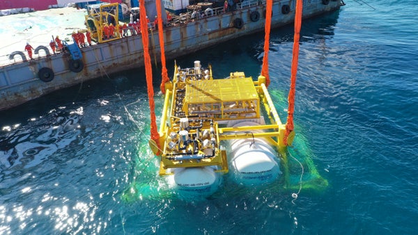
The underwater data center pictured here was a pilot project off the coast of Hainan. Another, more advanced, one is now being built off Shanghai.
Shanghai Hailanyun Technology
Artificial Intelligence
To grow its economy, China is betting big on artificial intelligence, cloud computing and other digital technology—and a big part of that bet involves rapidly building data centers to boost computing power. But these massive collections of servers gobble up growing amounts of energy, and each one cycles through hundreds of thousands of gallons of water a day to carry away the heat they generate.
You are outdated
China Is Putting Data Centers in the Ocean to Keep Them Cool
China is pulling ahead of the rest of the world in sinking data centers that power AI into the ocean as an alternate way to keep them cool
By You Xiaoying edited by Andrea Thompson
The underwater data center pictured here was a pilot project off the coast of Hainan. Another, more advanced, one is now being built off Shanghai.
Shanghai Hailanyun Technology
Artificial Intelligence
To grow its economy, China is betting big on artificial intelligence, cloud computing and other digital technology—and a big part of that bet involves rapidly building data centers to boost computing power. But these massive collections of servers gobble up growing amounts of energy, and each one cycles through hundreds of thousands of gallons of water a day to carry away the heat they generate.
This is reason why AMDK cannot agree with China, China has no respect for marine life and global warming
- Joined
- Sep 22, 2008
- Messages
- 98,335
- Points
- 113
All Those days centres spewing out millions of tons of co2 a day.This is reason why AMDK cannot agree with China, China has no respect for marine life and global warming
There is one planned as big as Manhattan but only employ few thousand workers. Compared to. Manhattan which employ millions.
- Joined
- Mar 3, 2024
- Messages
- 8,848
- Points
- 113
All the NWO nations can hide their AI data centers in Antarctica where sheeple can’t access at all. Putting data centers in underwater is likely a hoax and more likely, you have “believe” itYou are outdated
China Is Putting Data Centers in the Ocean to Keep Them Cool
China is pulling ahead of the rest of the world in sinking data centers that power AI into the ocean as an alternate way to keep them cool
By You Xiaoying edited by Andrea Thompson
The underwater data center pictured here was a pilot project off the coast of Hainan. Another, more advanced, one is now being built off Shanghai.
Shanghai Hailanyun Technology
Artificial Intelligence
To grow its economy, China is betting big on artificial intelligence, cloud computing and other digital technology—and a big part of that bet involves rapidly building data centers to boost computing power. But these massive collections of servers gobble up growing amounts of energy, and each one cycles through hundreds of thousands of gallons of water a day to carry away the heat they generate.
All their secret projects are in Antarctica

- Joined
- Jul 25, 2008
- Messages
- 65,638
- Points
- 113
pudding is in the money or money is in the pudding. just follow the money trail. wealthy tiongs are placing their massive bets on overseas stocks especially sillycon valley tech stocks hoping to siphon their funds out of tiongcock and stash them in high stakes stocks in the u.s. due to the surging u.s. stock market especially in ai tech, ccp cracks down on 3 online platforms in tiongcock that find ways and means for wealthy tiongs to do cross border trades with capital flight mainly to the u.s. stock market. many of these tiongs are anticipating 3 ipos this year on nasdaq: spacex, anthropic, openai. and many are buying up pre-ipo positions including some older pubic stocks that benefit from the ai data center buildout like bloom, micron, sandisk, cisco. this huawei bs no wealthy tiongs are interested except ccp cocksuckers and prc propaganda porlumpars.
Last edited:

- Joined
- Jun 17, 2020
- Messages
- 17,495
- Points
- 113
it will affect marine life and the marine ecosystem negatively. Pls dun do data centers.You are outdated
China Is Putting Data Centers in the Ocean to Keep Them Cool
China is pulling ahead of the rest of the world in sinking data centers that power AI into the ocean as an alternate way to keep them cool
By You Xiaoying edited by Andrea Thompson
The underwater data center pictured here was a pilot project off the coast of Hainan. Another, more advanced, one is now being built off Shanghai.
Shanghai Hailanyun Technology
Artificial Intelligence
To grow its economy, China is betting big on artificial intelligence, cloud computing and other digital technology—and a big part of that bet involves rapidly building data centers to boost computing power. But these massive collections of servers gobble up growing amounts of energy, and each one cycles through hundreds of thousands of gallons of water a day to carry away the heat they generate.

- Joined
- Jul 25, 2008
- Messages
- 65,638
- Points
- 113
on the surface reject nvidia for face and pride but underground smuggle in billions of nvidia chips for rebranding and reverse engineering. it’s a notorious strategy of ccp everyone in sillycon valley knows about sexcept you. if still clueless, can ask ceo, coo and cfo of supermicro in san jose. the billions of dollars of supermicro servers shipped to tiongcock via ccp-owned trading and distribution shell companies in sg contain nvidia blackwell chips. just kena busted by federal agents. cofounder kena arrested and indicted. very soon other cofounder will be indicted too. that so called “south east asian” company in the report is a sg based company.Regardless of whether the manufacturing process is overestimated, the recent rejection of a high-end nVidia chip serves as a testament to China's capabilities in developing its own AI-specific chip.
https://fortune.com/2026/03/19/supermicro-arrested-founder-smuggling-gpu-china/
Last edited:
Similar threads

- Replies
- 3
- Views
- 1K

- Replies
- 37
- Views
- 3K
- Replies
- 3
- Views
- 630


- Replies
- 1
- Views
- 719

